Lithium niobate (LiNbO₃, LN) has become an important functional material for radio-frequency, microwave, acoustic-wave, and electro-optic devices. Its combination of strong piezoelectric behavior, electro-optic response, wide optical transparency range, and mature wafer-processing compatibility makes lithium niobate wafers suitable for applications ranging from RF filters and surface acoustic wave devices to microwave photonics and high-speed optical modulators.
As wireless communication systems move toward higher frequencies, wider bandwidths, and more compact device architectures, the properties of the substrate become increasingly important. Selecting the appropriate LiNbO₃ wafer orientation, thickness, surface quality, and wafer structure can directly influence device performance and manufacturing stability.
This article explains how lithium niobate wafers are used in RF and microwave systems, what properties make them valuable, and what engineers should consider when selecting wafers for device development or volume production.
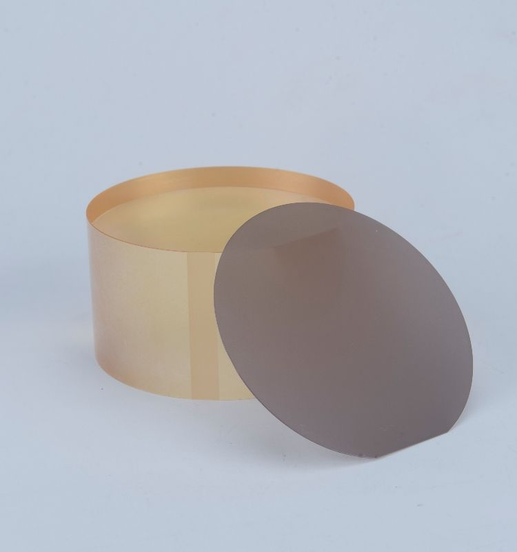
A lithium niobate wafer is a crystalline substrate manufactured from single-crystal lithium niobate. Depending on the application, the wafer may be supplied as a conventional bulk LiNbO₃ substrate or as part of a thin-film structure such as lithium niobate on insulator (LNOI).
Lithium niobate belongs to the ferroelectric crystal family and exhibits several useful physical effects, including:
Piezoelectric effect
Electro-optic effect
Nonlinear optical response
Acousto-optic interaction
Pyroelectric behavior
For RF applications, its piezoelectric properties are particularly important because electrical signals can be efficiently converted into acoustic waves and vice versa.
For microwave photonics and optical communication systems, lithium niobate's electro-optic properties allow high-speed electrical signals to control optical signals.
These characteristics allow a single material platform to support both electronic and photonic signal-processing technologies.
RF devices increasingly need to operate with higher frequency, lower signal loss, wide bandwidth, and good temperature and frequency stability.
Lithium niobate offers several characteristics that make it attractive for acoustic RF devices.
LiNbO₃ has relatively strong electromechanical coupling compared with many conventional piezoelectric substrates.
In an acoustic RF device, electrical energy applied through patterned electrodes generates mechanical acoustic waves inside or along the surface of the crystal.
Strong coupling can help engineers achieve:
Wider filter bandwidth
Efficient signal conversion
Compact device structures
Improved acoustic transducer performance
This is particularly valuable in modern RF front-end architectures where filters need to handle increasingly wide communication bands.
One of the most established RF applications of lithium niobate is the surface acoustic wave (SAW) device.
SAW devices generate acoustic waves that travel along the surface of a piezoelectric substrate. Interdigital transducers patterned on the wafer convert RF electrical signals into acoustic waves and then convert them back into electrical signals.
LiNbO₃ wafers can be used for manufacturing:
SAW filters
SAW resonators
RF delay lines
Acoustic sensors
Frequency-control devices
Wireless communication components
Because acoustic velocity and electromechanical coupling depend strongly on crystal orientation, wafer cut selection becomes an important part of SAW device design.
The lithium niobate industry increasingly uses two different substrate architectures.
| Wafer Type | Typical Characteristics | Common Applications |
|---|---|---|
| Bulk LiNbO₃ Wafer | Relatively thick single-crystal substrate | SAW devices, sensors, traditional optical devices |
| Thin-Film LiNbO₃ | Thin LiNbO₃ layer integrated with another substrate | High-frequency acoustic devices, integrated photonics |
| LNOI Wafer | Thin LiNbO₃ layer on dielectric isolation layer | Electro-optic modulators, photonic integrated circuits, microwave photonics |
Bulk wafers remain important for established SAW manufacturing and many industrial acoustic devices.
Thin-film lithium niobate, however, enables much stronger confinement of acoustic or optical energy and can support device structures that are difficult to achieve using conventional bulk substrates.
Lithium niobate on insulator (LNOI) typically consists of a thin single-crystal LiNbO₃ layer bonded to an insulating layer and supporting substrate.
The thin-film structure allows engineers to confine acoustic or optical fields more tightly within the lithium niobate layer.
For RF applications, this can support the development of:
High-frequency acoustic resonators
Wide-band RF filters
Thin-film acoustic devices
Microwave signal processors
Integrated RF-photonic systems
Thin-film LN technologies are especially attractive when device miniaturization and high-frequency operation are required.
RF filters are a critical part of modern wireless communication systems.
They separate desired communication bands from nearby signals and interference.
As wireless systems use more frequency bands, RF front-end modules need increasingly sophisticated filters with:
Wide bandwidth
High selectivity
Compact footprint
Low insertion loss
High operating frequency
Stable production characteristics
Lithium niobate's strong piezoelectric coupling makes it an important material for acoustic-wave filter development.
Potential applications include:
Cellular communication
5G RF front ends
Wi-Fi systems
IoT devices
Satellite communication equipment
Industrial wireless networks
The exact wafer orientation and structure depend on the filter architecture and target frequency band.
Lithium niobate is also important in systems operating in microwave frequency ranges.
Applications extend beyond conventional acoustic filters.
LiNbO₃ can be used in:
Piezoelectric and electro-optic structures can be designed to manipulate microwave-frequency signals.
Possible functions include:
Filtering
Delay
Frequency control
Modulation
Signal conversion
Microwave photonics combines RF and microwave electronics with optical systems.
Instead of processing high-frequency electrical signals entirely in electronic circuits, some microwave signals can be converted into or carried by optical signals.
Lithium niobate is particularly valuable because of its strong electro-optic effect.
Typical functions include:
RF-to-optical modulation
Optical transmission of microwave signals
Photonic microwave signal processing
Frequency conversion
High-speed communication links
One of the best-known applications of lithium niobate is the electro-optic modulator.
When an electric field is applied to lithium niobate, its refractive index changes. This allows the optical phase or intensity of light traveling through a waveguide to be controlled electrically.
Lithium niobate modulators are widely used in:
Fiber-optic communication
Microwave photonics
Optical sensing
Coherent communication systems
Scientific instrumentation
Photonic signal processing
Thin-film lithium niobate technology has enabled increasingly compact electro-optic devices while retaining the intrinsic electro-optic advantages of the crystal.
RF systems also use acoustic resonators as frequency-selective components.
A resonator stores acoustic energy at specific frequencies. The mechanical and electrical characteristics of the piezoelectric substrate strongly influence resonance behavior.
LiNbO₃ can support different acoustic modes depending on:
Crystal orientation
Film thickness
Electrode geometry
Propagation direction
Supporting substrate
Device structure
Thin-film lithium niobate has increased interest in new classes of acoustic resonators designed for higher frequencies and larger bandwidths.
Choosing a wafer based only on diameter is usually insufficient for RF device manufacturing.
Engineers should evaluate several parameters.
Crystal orientation affects:
Acoustic-wave propagation
Electromechanical coupling
Electro-optic interaction
Device polarization
Resonance characteristics
The correct cut depends on the specific RF or photonic device.
The required wafer diameter depends on device fabrication equipment and production scale.
Larger wafers may offer manufacturing advantages when processing infrastructure supports them, while smaller wafers remain common for R&D, prototyping, and specialized production.
Wafer thickness can influence mechanical handling, acoustic behavior, device integration, and downstream processing.
For bulk substrates, thickness must be compatible with lithography and wafer-handling equipment.
For thin-film LN, the thickness of the functional LiNbO₃ layer becomes an important design parameter because it can directly influence acoustic or optical confinement.
High-quality device fabrication requires good wafer surface conditions.
Important factors can include:
Surface roughness
Scratch control
Particle contamination
Polishing quality
Surface defects
For fine photonic waveguides and high-frequency RF structures, surface quality becomes particularly important.
Uniform wafer thickness helps maintain consistent processing conditions across the wafer.
Thickness variation may influence:
Lithography
Thin-film deposition
Etching
Bonding
Acoustic device frequency consistency
For volume RF component production, wafer uniformity becomes important for improving device-to-device repeatability.
Wafer bow and flatness affect compatibility with semiconductor manufacturing equipment.
Excessive bow may cause difficulties during:
Photolithography
Coating
Wafer bonding
Plasma processing
Automated handling
RF device manufacturers should therefore specify dimensional and flatness requirements according to their process flow.
Lithium niobate can be produced with different material compositions.
Two commonly discussed forms are:
Congruent lithium niobate
Stoichiometric lithium niobate
Congruent LiNbO₃ is widely used commercially because of established crystal-growth processes.
Stoichiometric lithium niobate has a composition closer to the ideal lithium-to-niobium ratio and can offer different optical and electrical properties.
The appropriate material depends on the target application and required device characteristics.
For many RF acoustic applications, orientation, wafer structure, acoustic behavior, and fabrication compatibility may be more directly relevant purchasing parameters.
Lithium niobate crystals may also be doped with selected elements to modify certain material properties.
For example, doped materials may be evaluated in optical applications where resistance to optical damage or other specific characteristics are required.
However, doping should not be treated as universally beneficial.
For RF and microwave devices, engineers should first determine whether the dopant improves the required acoustic, electrical, or optical behavior.
Depending on device manufacturing requirements, lithium niobate wafers may be supplied with different polishing configurations.
One surface is prepared for device processing while the opposite side may remain less highly finished.
This configuration may be suitable for certain acoustic, sensor, or research applications.
Both surfaces are polished.
Double-side polishing may be required for applications involving:
Optical transmission
Wafer bonding
Backside processing
Thin-film integration
Advanced photonic fabrication
The wafer supplier should understand the customer's downstream process before recommending the appropriate polishing configuration.
In many RF acoustic devices, metallic interdigital transducers are patterned directly on the lithium niobate surface.
Typical fabrication steps may include:
Wafer cleaning
Photoresist coating
Lithographic patterning
Metal deposition
Lift-off or etching
Electrical testing
Wafer dicing
The electrode pitch and geometry determine important characteristics of the acoustic device, including operating frequency.
As RF frequencies increase, electrode dimensions may become smaller, placing greater demands on wafer surface quality and lithographic process control.
A wafer is not simply a mechanical support.
In piezoelectric RF devices, it is an active part of the device.
Variations in substrate properties can lead to variations in:
Resonant frequency
Acoustic velocity
Coupling behavior
Device impedance
Filter response
For commercial RF production, manufacturers therefore pay close attention to batch-to-batch and wafer-to-wafer consistency.
Important quality-control parameters may include:
Crystal orientation accuracy
Thickness tolerance
Diameter tolerance
Surface roughness
Flatness
Bow
Edge condition
Defect control
Reliable wafer specifications can help downstream manufacturers achieve more stable fabrication processes.
5G and next-generation wireless systems require more complex RF front-end architectures because mobile devices and infrastructure systems must support increasing numbers of frequency bands.
This creates demand for filter technologies capable of combining:
Higher operating frequencies
Wider bandwidth
Compact size
Low power loss
High signal isolation
The strong piezoelectric properties of LiNbO₃ and the growing development of thin-film lithium niobate structures have made the material an important research and commercial platform for advanced RF components.
Although wireless communication is an important market, lithium niobate wafers are used in many other technologies.
SAW structures can detect changes in:
Pressure
Temperature
Mass loading
Chemical environment
This allows LiNbO₃ substrates to be used in various sensing applications.
Acoustic devices may be incorporated into wireless sensor or identification systems where passive or remotely interrogated operation is desirable.
Lithium niobate devices are widely used in optical and microwave laboratories for modulation, frequency control, and signal-processing experiments.
RF filtering, microwave photonics, and high-frequency signal-processing technologies can also require advanced piezoelectric and electro-optic materials.
The exact substrate specification depends on environmental, electrical, and reliability requirements.
Lithium niobate wafers for RF and microwave applications provide a versatile material platform combining strong piezoelectric and electro-optic properties.
Traditional bulk LiNbO₃ wafers continue to support established technologies such as SAW filters, resonators, acoustic sensors, and frequency-control devices, while thin-film lithium niobate and LNOI are expanding the possibilities for high-frequency acoustic devices, microwave photonics, and integrated electro-optic systems.
For device manufacturers, selecting the right wafer requires careful consideration of crystal orientation, thickness, surface quality, flatness, polishing method, and wafer architecture.
Working with a lithium niobate wafer supplier capable of controlling crystal orientation and precision wafer processing can help RF component developers move more efficiently from laboratory evaluation to stable production.



Copyright © Hangzhou Freqcontrol
Electronic Technology Ltd.
All Rights Reserved | Sitemap |
Powered by 







 中文
中文


