The rapid evolution of wireless communication technologies—including 5G, Wi-Fi 6/6E, Wi-Fi 7, IoT, satellite communication, automotive radar, and advanced mobile devices—has significantly increased the demand for high-performance radio frequency (RF) filters and resonators. Among the key materials enabling these technologies, Lithium Niobate Wafers (LiNbO₃) stand out for their exceptional piezoelectric and electro-acoustic properties.
Lithium niobate is widely used as a substrate for Surface Acoustic Wave (SAW) devices and is increasingly being explored in Bulk Acoustic Wave (BAW) and thin-film acoustic technologies due to its high electromechanical coupling coefficient, excellent crystal quality, and stable performance.
In this guide, we'll explore why lithium niobate wafers are ideal for SAW and BAW devices, key selection criteria, common specifications, and procurement considerations for RF manufacturers.
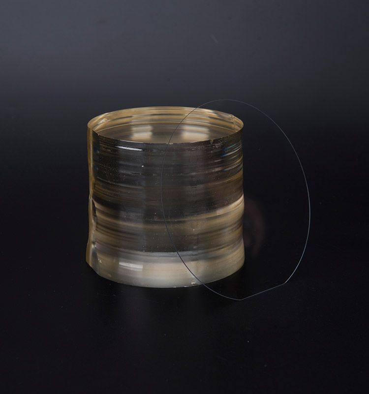
Lithium niobate (LiNbO₃) is a synthetic single-crystal material with unique electro-optic, piezoelectric, ferroelectric, and nonlinear optical properties. It has become one of the most widely used functional crystal materials in modern electronics and photonics.
Its outstanding piezoelectric characteristics make it particularly suitable for acoustic wave devices that convert electrical signals into mechanical waves and vice versa.
What Is a SAW Device?
A Surface Acoustic Wave (SAW) device transmits acoustic waves along the surface of a piezoelectric substrate.
Common SAW components include:
RF Filters
Duplexers
Resonators
Delay Lines
Oscillators
Sensors
SAW technology is widely used because it offers:
Compact size
Low insertion loss
Excellent frequency stability
Cost-effective manufacturing
What Is a BAW Device?
Bulk Acoustic Wave (BAW) devices generate acoustic waves that travel through the thickness of the material rather than along the surface.
Typical BAW technologies include:
FBAR (Film Bulk Acoustic Resonator)
SMR (Solidly Mounted Resonator)
BAW filters are preferred for:
Higher operating frequencies
Better power handling
Wider bandwidth
Lower signal interference
Although aluminum nitride (AlN) is commonly used in commercial BAW filters, lithium niobate thin-film technologies are attracting significant attention for next-generation RF applications because of their superior electromechanical coupling.
Lithium niobate provides several advantages over many traditional piezoelectric materials.
High Electromechanical Coupling Coefficient
One of lithium niobate's greatest strengths is its exceptionally high electromechanical coupling coefficient (K²).
Benefits include:
Higher filter bandwidth
Better signal conversion efficiency
Improved RF performance
Lower insertion loss
This is especially important in modern 5G communication systems.
Excellent Piezoelectric Performance
Lithium niobate efficiently converts:
Electrical Energy ⇄ Mechanical Acoustic Waves
This enables:
High sensitivity
Stable signal transmission
Low distortion
Fast response
Low Acoustic Loss
High-quality lithium niobate crystals provide:
Reduced propagation loss
Higher Q-factor
Better frequency stability
Improved filter efficiency
Outstanding Frequency Stability
Lithium niobate wafers exhibit stable performance across varying operating conditions.
Advantages include:
Reliable RF filtering
Consistent resonator performance
Long operational lifetime
Mature Manufacturing Technology
Lithium niobate crystal growth has been optimized over decades.
Manufacturers can provide:
High crystal uniformity
Low defect density
Excellent wafer flatness
Precision polishing
Large-diameter wafers
Consistent batch quality
Lithium niobate is one of the most common substrate materials for SAW components.
Typical applications include:
RF Filters
Used in:
Smartphones
Tablets
Base stations
Wireless routers
IoT modules
Duplexers
Enable simultaneous transmission and reception in wireless systems.
Applications:
4G LTE
5G NR
Satellite communication
SAW Resonators
Provide:
Stable frequency control
Low phase noise
High reliability
Delay Lines
Widely used in:
Radar systems
Signal processing
Test equipment
SAW Sensors
Suitable for:
Pressure sensing
Temperature monitoring
Chemical detection
Industrial automation
Automotive systems
Although traditional BAW filters typically use aluminum nitride, Thin-Film Lithium Niobate (TFLN) is becoming an attractive alternative.
Advantages include:
Higher electromechanical coupling
Wider filter bandwidth
Improved RF efficiency
Better support for high-frequency communication
Compatibility with integrated RF modules
Research continues to accelerate in:
5G mmWave
6G communication
Advanced RF front-end modules
Microwave integrated circuits
Wafer Diameter
Available sizes typically include:
2 inch
3 inch
4 inch
6 inch (customized)
Larger wafers improve production efficiency for volume manufacturing.
Wafer Thickness
Typical thicknesses:
350 μm
500 μm
700 μm
Customized
Thickness should match fabrication processes and equipment requirements.
Surface Finish
High-quality polishing ensures:
Uniform lithography
Better electrode deposition
Reduced acoustic scattering
Higher production yield
Common options include:
Single-side polished (SSP)
Double-side polished (DSP)
Crystal Quality
Look for wafers with:
Low dislocation density
Minimal inclusions
Excellent optical uniformity
Stable crystal domains
Low internal stress
Higher crystal quality leads to more consistent RF device performance.
Several wafer characteristics affect final device quality.
Surface Roughness
Ultra-smooth surfaces improve:
Acoustic propagation
Electrode adhesion
Manufacturing precision
Wafer Flatness
Excellent flatness provides:
Better lithography accuracy
Uniform film deposition
Higher device consistency
Orientation Accuracy
High orientation precision ensures:
Stable resonant frequency
Consistent acoustic velocity
Better manufacturing repeatability
Temperature Stability
Proper crystal selection improves:
Frequency stability
Environmental reliability
Long-term operation
When evaluating suppliers, consider the following capabilities:
Crystal Growth Expertise
A reputable manufacturer should maintain strict control over:
Crystal purity
Growth process
Material consistency
Precision Processing
Look for suppliers offering:
Precision cutting
High-quality polishing
Orientation customization
Edge grinding
Wafer cleaning
Quality Control
Reliable suppliers provide:
Dimensional inspection
Crystal orientation reports
Surface roughness measurements
Flatness testing
Material certifications
Custom Manufacturing
Many RF manufacturers require custom specifications, including:
Special orientations
Customized thickness
Double-side polishing
Edge profile options
Unique packaging solutions
Avoid these common purchasing errors:
Selecting the wrong crystal orientation
Ignoring electromechanical performance
Focusing only on price
Overlooking surface quality
Not requesting inspection reports
Choosing suppliers without stable production capability
Ignoring customization requirements
Proper supplier evaluation can significantly improve manufacturing yield and reduce production risks.
The demand for lithium niobate wafers continues to grow alongside the expansion of wireless communication technologies.
Key market trends include:
Growth of 5G and future 6G infrastructure
Expansion of Wi-Fi 7 networks
Increased adoption of RF front-end modules
Development of thin-film lithium niobate (TFLN)
Advanced acoustic resonator technologies
Miniaturization of communication devices
Integration of acoustic and photonic components
Higher-frequency RF filter solutions
These trends are expected to drive continued innovation in lithium niobate wafer manufacturing and acoustic device design.
Lithium Niobate Wafers remain one of the most important substrate materials for SAW devices and are gaining momentum in next-generation BAW and thin-film acoustic applications. Their high electromechanical coupling, outstanding piezoelectric properties, low acoustic loss, and mature manufacturing processes make them a preferred choice for RF filters, resonators, sensors, and communication components.
When selecting a wafer, manufacturers should carefully evaluate crystal orientation, surface quality, wafer dimensions, flatness, and supplier expertise. Working with an experienced supplier that offers consistent crystal quality, precision processing, and customization services can help improve device performance, manufacturing efficiency, and long-term reliability.



Copyright © Hangzhou Freqcontrol
Electronic Technology Ltd.
All Rights Reserved | Sitemap |
Powered by 







 中文
中文


