As integrated photonics continues to reshape industries such as telecommunications, quantum computing, LiDAR, optical sensing, and high-speed data transmission, Lithium Niobate Wafers have become one of the most important substrate materials for advanced photonic devices. Their exceptional electro-optic, nonlinear optical, piezoelectric, and acousto-optic properties make them the preferred choice for researchers, semiconductor manufacturers, and photonic component suppliers worldwide.
However, selecting the right lithium niobate wafer is not simply a matter of choosing a diameter or thickness. Crystal orientation, composition, surface quality, optical grade, wafer flatness, and supplier capabilities all directly influence device performance, production yield, and long-term reliability.
This guide explains everything procurement engineers, R&D teams, and photonics manufacturers should consider when purchasing Lithium Niobate Wafers for photonics applications.
Lithium niobate (LiNbO₃) is often referred to as the "silicon of photonics" because of its outstanding electro-optic characteristics.
Major advantages include:
High electro-optic coefficient
Excellent optical transparency (350 nm–5.2 μm)
Low optical absorption
Strong nonlinear optical performance
Stable physical and chemical properties
High Curie temperature
Excellent piezoelectric properties
Mature crystal growth technology
Compatibility with integrated photonic fabrication
These characteristics make lithium niobate indispensable for modern optical systems.
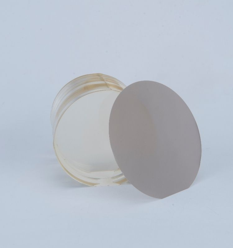
Lithium niobate wafers are widely used in:
Optical modulators
Optical switches
Waveguides
Frequency converters
Optical communication systems
Quantum photonics
Integrated photonic chips
Laser frequency doubling
Electro-optic sensors
Microwave photonics
Acousto-optic devices
Optical signal processing
LiDAR systems
Fiber optic communication
Photonic integrated circuits (PIC)
Before choosing a wafer, clearly define your application.
Different applications require different wafer specifications.
Crystal orientation has a significant impact on device performance.
The most common orientations include:
X-Cut Lithium Niobate Wafers
Suitable for:
Electro-optic modulators
Optical communication
Thin-film lithium niobate devices
Advantages:
Excellent electro-optic efficiency
Widely used in photonic integrated circuits
High modulation performance
Y-Cut Lithium Niobate Wafers
Ideal for:
Surface acoustic wave (SAW) devices
Piezoelectric applications
RF filters
Advantages:
Superior acoustic performance
Excellent piezoelectric response
Z-Cut Lithium Niobate Wafers
Commonly used for:
Nonlinear optics
Optical waveguides
Frequency conversion
Laser applications
Advantages:
High nonlinear coefficient
Stable optical properties
One of the most important purchasing decisions involves crystal composition.
Congruent Lithium Niobate (CLN)
Characteristics:
Most widely available
Cost-effective
Mature manufacturing process
Suitable for general photonics
Applications:
Optical modulators
Commercial photonic devices
Optical communication
Stoichiometric Lithium Niobate (SLN)
Characteristics:
Higher optical quality
Lower defect density
Better resistance to photorefractive damage
Improved nonlinear efficiency
Applications:
High-power lasers
Quantum optics
Precision photonic devices
Although SLN costs more, it often provides superior performance in demanding applications.
Available diameters typically include:
2 inch
3 inch
4 inch
6 inch (Thin-film applications)
Larger wafers provide:
Higher production efficiency
Better compatibility with semiconductor fabrication
Lower manufacturing cost per device
However, they require more advanced processing capabilities.
Surface polishing directly impacts optical device performance.
Important specifications include:
Single-side polished (SSP)
Double-side polished (DSP)
Surface roughness (Ra)
Scratch/Dig quality
Surface defects
Micro-cracks
Edge chipping
High-end photonic devices usually require double-side polished wafers with ultra-low surface roughness.
High-quality crystals improve fabrication yield.
Important inspection items include:
Crystal uniformity
Inclusion density
Dislocation density
Optical homogeneity
Internal stress
Domain quality
Lower defect density generally leads to:
Better optical transmission
Lower insertion loss
Higher device reliability
Depending on your application, doped lithium niobate may offer significant advantages.
Popular options include:
MgO-Doped Lithium Niobate
Benefits:
Improved resistance to photorefractive damage
Better high-power laser performance
Enhanced stability
Applications:
High-power optics
Frequency conversion
Laser systems
Fe-Doped Lithium Niobate
Applications:
Holographic storage
Optical data recording
Photorefractive research
Zn-Doped Lithium Niobate
Advantages:
Improved optical properties
Enhanced photorefractive resistance
Professional buyers should review:
Refractive index uniformity
Optical transmission
Absorption coefficient
Birefringence consistency
Optical homogeneity
These parameters directly affect photonic device efficiency.
A trustworthy supplier should provide:
ISO-certified manufacturing
Complete material traceability
Advanced crystal growth technology
Precision polishing capability
Custom wafer processing
Strict quality inspection
Technical support
Stable production capacity
Ask whether the supplier offers:
Orientation customization
Diameter customization
Thickness customization
Edge profile options
Surface finish customization
Cleaning and packaging services
Many buyers focus only on price while overlooking technical specifications.
Common mistakes include:
Choosing the wrong crystal orientation
Ignoring surface quality
Overlooking wafer flatness
Not verifying crystal composition
Purchasing from suppliers without quality certifications
Ignoring optical uniformity
Selecting unsuitable thickness
Failing to request inspection reports
Avoiding these mistakes can significantly improve production yield.
Before placing an order, ask your supplier:
Is the wafer congruent or stoichiometric?
What crystal orientation is available?
What polishing process is used?
What is the surface roughness?
Are inspection reports provided?
What is the wafer flatness tolerance?
Are custom specifications supported?
What packaging method prevents contamination?
Can you provide application engineering support?
What is the production lead time?
The rapid development of photonic integrated circuits is driving demand for advanced lithium niobate substrates.
Emerging trends include:
Thin-film lithium niobate (TFLN)
Ultra-low-loss photonic chips
Co-packaged optics
Silicon-lithium niobate hybrid integration
Quantum communication
AI data center optical interconnects
High-speed 800G and 1.6T optical modules
Next-generation LiDAR systems
As these technologies mature, high-quality lithium niobate wafers will remain a foundational material for the photonics industry.
Choosing the right Lithium Niobate Wafers for photonics applications requires a careful evaluation of crystal orientation, composition, diameter, thickness, surface quality, optical properties, and supplier expertise. While cost is an important consideration, long-term device performance, manufacturing yield, and reliability depend on selecting wafers that precisely match your application's technical requirements.
Partnering with an experienced manufacturer that offers consistent crystal quality, precision processing, and customization services can help ensure your photonic devices achieve optimal performance while reducing production risks.



Copyright © Hangzhou Freqcontrol
Electronic Technology Ltd.
All Rights Reserved | Sitemap |
Powered by 







 中文
中文


