As electronic and photonic systems continue to shrink in size while demanding higher performance, material innovation has become a key driver of progress. Thin-film lithium niobate has emerged as a transformative solution, enabling a new generation of compact, high-speed, and energy-efficient devices. By combining the exceptional properties of lithium niobate with advanced thin-film fabrication techniques, this material is redefining what is possible in device miniaturization.
Thin-film lithium niobate refers to ultra-thin layers of lithium niobate bonded or deposited onto a supporting substrate, typically silicon or an insulating layer. Unlike bulk lithium niobate wafers, thin-film structures allow for precise control of optical and electrical confinement, significantly enhancing device performance while reducing overall size.
This platform is often fabricated using advanced processes such as ion slicing, wafer bonding, and layer transfer technologies, resulting in high-quality crystalline films with thicknesses ranging from a few hundred nanometers to several micrometers.
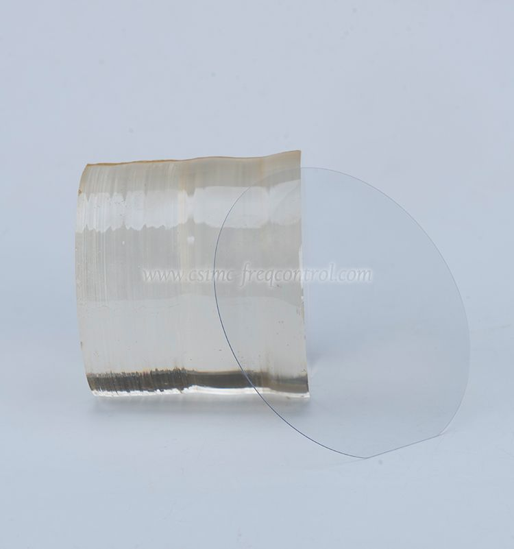
Lithium niobate has long been valued for its:
Strong electro-optic effect
High piezoelectric response
Wide optical transparency range
Excellent thermal and chemical stability
However, traditional bulk lithium niobate components are relatively large and difficult to integrate into compact systems. Thin-film technology overcomes these limitations by enabling tighter optical confinement and higher integration density.
1. Significant Size Reduction
Thin-film structures allow devices to be fabricated on a much smaller scale compared to bulk materials. Waveguides, modulators, and acoustic components can be integrated into compact chip-scale platforms.
2. Enhanced Electro-Optic Efficiency
Stronger light confinement in thin films increases the interaction between optical signals and the electric field, leading to lower driving voltage and higher modulation efficiency.
3. High-Speed Performance
Thin-film lithium niobate supports ultra-fast signal processing, making it ideal for high-frequency communication systems and data transmission applications.
4. Lower Power Consumption
Improved efficiency reduces the required driving power, which is critical for portable and high-density electronic devices.
5. Integration with Silicon Platforms
Thin-film lithium niobate can be integrated with silicon photonics, enabling hybrid devices that combine the strengths of both materials.
Thin-film lithium niobate is enabling breakthroughs across multiple industries:
Optical Modulators
Compact, high-speed modulators for data centers, fiber-optic communication, and coherent transmission systems
Surface Acoustic Wave Devices
Miniaturized filters and resonators for wireless communication and radio frequency front-end modules
Photonic Integrated Circuits
Integration of multiple optical functions on a single chip for advanced signal processing
Sensors and Precision Instruments
High-sensitivity sensing devices with reduced size and improved performance
Quantum and Nonlinear Optics
Platforms for frequency conversion, quantum information processing, and advanced photonic research
While thin-film lithium niobate offers significant advantages, there are still challenges to address:
Complex fabrication processes
Higher production costs compared to bulk materials
Integration challenges with existing manufacturing ecosystems
Ongoing research and industrial scaling are steadily reducing these barriers.
Thin-film lithium niobate is poised to play a central role in the future of miniaturized devices:
Expansion in high-speed communication systems
Increased adoption in photonic integrated circuits
Growth in quantum and nonlinear optical applications
Continued improvements in fabrication efficiency and cost
As industries push toward smaller, faster, and more efficient systems, thin-film lithium niobate will remain a key enabling material.
Thin-film lithium niobate is revolutionizing device miniaturization by combining the proven advantages of lithium niobate with modern thin-film engineering. Its ability to deliver high performance in a compact form factor makes it a critical material for next-generation electronics and photonics.
From optical communications to advanced sensing and integrated photonics, thin-film lithium niobate is shaping the future of high-performance, miniaturized technologies.



Copyright © Hangzhou Freqcontrol
Electronic Technology Ltd.
All Rights Reserved | Sitemap |
Powered by 







 中文
中文


