Lithium Niobate Wafers are used in optical modulators, RF filters, acoustic devices, piezoelectric sensors, and integrated photonics. Selecting the correct wafer is not only a matter of comparing diameter and price. Purchasing teams also need technical support that translates application requirements into measurable wafer specifications, verifies supplier capability, reduces qualification risk, and protects production schedules.
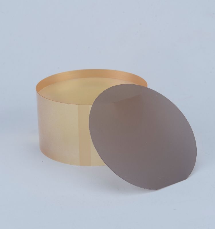
Why supplier technical support influences wafer selection
Technical support connects application requirements with wafer specifications
Purchasing teams often receive wafer requests with incomplete or unclear specifications. A device engineer may ask for a thin wafer, a low-loss surface, or a specific crystal cut without defining the full production requirements. An experienced supplier should help convert these terms into measurable parameters.
- Application type, such as optical, RF, SAW, BAW, MEMS, or sensor use.
- Crystal cut, including X-cut, Y-cut, Z-cut, or rotated cuts.
- Wafer diameter and usable area.
- Wafer thickness and thickness tolerance.
- Surface finish, roughness, and polishing method.
- Total thickness variation, bow, and warp.
- Resistivity, dielectric performance, or optical transmission requirements.
- Defect density, inclusions, scratches, particles, and edge quality.
- Packaging, cleanliness, traceability, and inspection documentation.
Support reduces the cost of choosing the wrong wafer
A low-priced wafer can create higher total costs if it causes device yield loss, extra process development, delayed qualification, or inconsistent performance between batches. Supplier support helps the purchasing group evaluate total cost instead of unit price alone.
- Lower risk of ordering an incompatible crystal orientation.
- Fewer engineering changes caused by incorrect thickness or surface specifications.
- Earlier identification of supply limitations and lead-time risks.
- More reliable comparison between supplier quotations.
- Better control of pilot-run and mass-production costs.
Purchasing teams need evidence, not general claims
Supplier technical support should be supported by inspection data, sample records, process explanations, and clear acceptance criteria. Statements such as high quality, premium material, or excellent uniformity are not sufficient for a technical purchasing decision.
Useful evidence includes:
- Certificate of analysis for each lot.
- Thickness, TTV, bow, and warp measurement results.
- Surface inspection images or inspection summaries.
- Crystal orientation verification.
- Material composition or stoichiometry information where relevant.
- Sample qualification records.
- Corrective action history and response procedures.
- Production capacity and lot-to-lot consistency data.
Start with an application-based wafer specification
First step: define the device and process requirements
Before contacting suppliers, the purchasing and engineering teams should create a basic application brief. This document prevents suppliers from making assumptions and gives all suppliers the same information for quotation and comparison.
- Identify the final device, such as an optical modulator, SAW filter, acoustic resonator, sensor, or photonic integrated circuit.
- Record the process flow, including deposition, lithography, etching, bonding, thinning, dicing, and packaging.
- Define the target electrical, optical, acoustic, or mechanical performance.
- List all wafer specifications that are mandatory and separate them from preferred specifications.
- Define the prototype quantity, qualification quantity, and expected annual volume.
- Set the required delivery date and acceptable lead-time range.
Second step: select the correct crystal cut and orientation
Crystal orientation directly affects piezoelectric coupling, optical response, etching behavior, thermal performance, and device integration. The supplier should explain why a proposed cut is suitable for the application instead of simply accepting a generic request.
- X-cut wafers can be selected for specific electro-optic and piezoelectric device configurations.
- Y-cut and Z-cut wafers may be preferred for different optical, acoustic, or sensor structures.
- Rotated cuts may be required to achieve a target coupling coefficient or frequency response.
- Orientation tolerance should be specified and verified by an agreed measurement method.
- Flat or notch orientation should match the equipment and wafer handling system.
Third step: confirm size, thickness, and usable area
Wafer diameter and thickness should be matched to the production equipment, handling tools, bonding process, and device layout. A nominal size alone does not show how much usable area will remain after edge exclusion and defect screening.
- Confirm the wafer diameter, such as 2 inch, 3 inch, 4 inch, or another required size.
- Confirm nominal thickness and thickness tolerance.
- Review edge exclusion requirements and usable device area.
- Check compatibility with chucks, carriers, cassettes, and bonding equipment.
- Confirm whether the supplier can maintain the same specification at higher volumes.
Fourth step: define surface and geometry requirements
Surface quality is often a major source of yield problems. The supplier should provide measurable limits for roughness, scratches, pits, stains, particles, TTV, bow, and warp.
- Specify single-side or double-side polishing.
- Define target surface roughness and measurement method.
- Set limits for scratches, pits, haze, particles, and edge chips.
- Define TTV, bow, and warp limits based on the process equipment.
- Confirm whether the wafer requires a specific cleaning or packaging standard.
Use a structured supplier technical support process
First step: send a complete technical inquiry
A complete inquiry allows the supplier to recommend a technically suitable wafer and reduces repeated clarification. The inquiry should contain both the current requirements and the intended development path.
- Application and device type.
- Crystal material and preferred cut.
- Wafer diameter and thickness.
- Surface finish and geometry limits.
- Required quantity for samples and production.
- Target performance and test method.
- Required certificates and inspection data.
- Expected delivery schedule.
- Forecasted annual demand.
Second step: ask the supplier to explain its recommendation
Do not only request a quotation. Ask the supplier to explain how each wafer parameter affects the device process. This reveals whether the supplier has practical technical knowledge or is only reselling standard material.
Important questions include:
- Why is the recommended crystal cut suitable for the application?
- How is orientation measured and what is the tolerance?
- What process controls are used to maintain thickness uniformity?
- How are surface defects detected and classified?
- What is the normal variation between lots?
- Which specifications are standard and which require custom processing?
- What changes occur when moving from sample quantity to production quantity?
- What technical support is available during device qualification?
Third step: review sample data before approving the supplier
Sample approval should be based on both wafer inspection and device process results. A wafer can meet a general specification but still perform poorly in a specific process.
- Review the supplier certificate and lot identification.
- Measure critical wafer parameters using internal equipment where possible.
- Run the planned process on a representative sample.
- Record yield, surface defects, bonding quality, etch behavior, and device performance.
- Compare the results with the agreed acceptance criteria.
- Document deviations and request corrective action before volume approval.
Fourth step: establish a technical escalation procedure
Purchasing teams need a clear communication path when wafers do not meet expectations. The supplier should identify a technical contact, a quality contact, and a management escalation contact.
- Define the response time for urgent technical questions.
- Define the format for nonconformance reports.
- Set the required root cause analysis timeline.
- Specify replacement, rework, or credit procedures.
- Record all approved specification changes in writing.
Compare suppliers using technical and commercial criteria
Use a weighted supplier evaluation matrix
A purchasing group should avoid selecting a supplier based only on quotation price. A weighted matrix makes the decision more transparent and allows engineering, quality, and procurement teams to evaluate the same suppliers.
| Evaluation category |
Key questions |
Suggested priority |
| Material and crystal quality |
Are cut, composition, defects, and optical or electrical properties consistent? |
Very high |
| Dimensional control |
Can the supplier maintain thickness, TTV, bow, warp, and diameter limits? |
High |
| Technical support |
Can the supplier help with specification definition, process issues, and qualification? |
Very high |
| Quality documentation |
Are inspection records, certificates, and traceability complete? |
High |
| Capacity and delivery |
Can the supplier support sample, pilot, and production volumes? |
High |
| Commercial terms |
Are price, payment, warranty, replacement, and shipping terms acceptable? |
Medium |
Check whether support continues after the purchase order
Some suppliers provide detailed assistance before an order but offer limited help after delivery. Purchasing teams should evaluate the complete support cycle.
- Pre-sales specification consultation.
- Sample selection and application guidance.
- Qualification support.
- Lot inspection and documentation.
- Failure analysis assistance.
- Process change notification.
- Production ramp-up support.
Evaluate total cost of ownership
Total cost includes more than the invoice price. It should include engineering time, incoming inspection, rejected wafers, process interruptions, requalification, expedited shipping, and device yield impact.
- Unit wafer price.
- Tooling or custom processing charges.
- Incoming inspection cost.
- Expected scrap and replacement cost.
- Qualification and engineering labor.
- Inventory required to protect against late delivery.
- Cost of production downtime caused by inconsistent material.
Required tools for wafer selection and supplier qualification
Technical specification tools
The following tools help the purchasing team and engineering team define requirements before supplier selection:
- Application requirement form.
- Wafer specification checklist.
- Process flow diagram.
- Device performance target sheet.
- Supplier comparison matrix.
- Approved vendor list template.
- Risk assessment and failure mode analysis form.
Inspection and measurement tools
Not every purchasing organization needs to own every instrument, but the inspection method should be available internally or through a qualified laboratory.
- Optical microscope for scratches, particles, edge chips, and surface contamination.
- Surface profiler or interferometer for roughness and surface form.
- Thickness gauge or calibrated micrometer for thickness verification.
- Wafer geometry measurement system for TTV, bow, and warp.
- Particle inspection system for cleanliness evaluation.
- Crystal orientation verification equipment or qualified external laboratory.
- Optical transmission, electrical, or acoustic test equipment when application performance must be verified.
- Cleanroom packaging and handling equipment for incoming inspection.
Documentation and communication tools
Good documentation prevents technical information from being lost between purchasing, engineering, quality, and the supplier.
- Controlled technical data sheet.
- Purchase specification attached to the purchase order.
- Lot traceability system.
- Nonconformance report template.
- Corrective action request template.
- Shared sample qualification report.
- Supplier performance dashboard.
Common purchasing mistakes to avoid
Mistake 1: selecting the lowest quotation without checking yield risk
A low price does not compensate for poor uniformity, inconsistent surface quality, or weak technical support. Compare suppliers using yield impact, replacement policy, documentation quality, and delivery reliability.
Mistake 2: using incomplete or ambiguous specifications
Terms such as optical grade, high quality, thin wafer, or low defect are open to interpretation. Replace them with numerical limits, inspection methods, sampling plans, and acceptance criteria.
Mistake 3: ignoring crystal orientation and process compatibility
Ordering the correct material with the wrong cut or orientation can make the wafer unsuitable for the intended device. Obtain written confirmation of orientation, tolerance, flat or notch direction, and verification method.
Mistake 4: approving samples without testing the real process
Visual inspection alone cannot confirm device performance. Use the same cleaning, bonding, deposition, lithography, etching, and measurement conditions planned for production.
Mistake 5: failing to distinguish sample capability from production capability
A supplier may produce a small number of excellent wafers but struggle to maintain the same quality at higher volume. Ask for capacity data, process control information, and a scale-up plan.
Mistake 6: accepting undocumented specification changes
Changes in raw material, polishing process, inspection method, packaging, or subcontractor can affect wafer performance. Require advance notification and requalification rules for material or process changes.
Mistake 7: treating technical support as a sales service only
Effective support should continue after delivery. Purchasing teams should confirm that the supplier can assist with defect investigation, lot comparison, process troubleshooting, and corrective action.
Build a step-by-step wafer selection workflow
First step: create the internal requirement sheet
- Collect requirements from device engineering, process engineering, quality, and production.
- Separate mandatory parameters from recommended parameters.
- Define measurable acceptance limits for every critical characteristic.
- Identify the risks associated with each parameter.
Second step: screen technically capable suppliers
- Review the supplier product range and available crystal cuts.
- Confirm wafer diameter, thickness, surface finish, and geometry capability.
- Review technical staff experience and communication quality.
- Check production capacity, quality systems, and traceability.
- Remove suppliers that cannot meet mandatory requirements.
Third step: request samples and supporting data
- Send the same controlled specification to each shortlisted supplier.
- Request sample wafers from identified production lots.
- Request certificates, inspection data, and packaging information.
- Ask each supplier to identify potential risks or recommended specification changes.
Fourth step: complete technical qualification
- Inspect incoming wafers using the approved measurement plan.
- Process the wafers using representative manufacturing conditions.
- Measure device performance and process yield.
- Compare results with the specification and internal baseline.
- Record all deviations and obtain written supplier responses.
Fifth step: complete commercial and supply qualification
- Compare total landed cost rather than unit price only.
- Confirm lead time, minimum order quantity, payment terms, and shipping conditions.
- Review replacement and nonconformance policies.
- Confirm forecast planning and capacity reservation options.
- Approve the supplier only after quality and supply risks are documented.
Sixth step: monitor performance after approval
- Track incoming inspection results for every lot.
- Monitor yield, defect trends, delivery performance, and response time.
- Review supplier performance at regular intervals.
- Requalify the supplier after significant material or process changes.
- Maintain a backup supplier for critical production programs.
Choose a supplier that supports long-term production
Look for application-focused communication
The best supplier does more than provide a catalog number. The supplier should ask about the device, process, equipment, performance target, and future volume before recommending a wafer. This approach helps the purchasing group avoid technically unsuitable alternatives.
Look for consistent quality and traceability
Every production lot should be identifiable and supported by appropriate inspection records. Consistent documentation makes it easier to compare lots, investigate failures, and maintain stable production.
Look for support from sample stage to mass production
A reliable supplier should provide a clear transition plan from prototype wafers to pilot production and volume supply. The plan should address specification control, capacity, lead time, packaging, inspection, and change notification.
CQT can support purchasing and engineering teams with application-based specification review, Lithium Niobate Wafers selection, sample qualification, technical documentation, and production supply planning. When supplier technical support is evaluated as part of quality and total cost, the purchasing decision becomes more reliable and easier to defend internally.
For projects that depend on stable optical, acoustic, electrical, or piezoelectric performance, choosing the right Lithium Niobate Wafers and the right technical partner is a direct investment in yield, delivery reliability, and long-term product performance.









 中文
中文


