Lithium Niobate Wafers are engineered crystal substrates used in optical communication, photonics, radio-frequency devices, sensors, and quantum technology. Their value comes from a useful combination of electro-optic, piezoelectric, nonlinear optical, and acousto-optic properties. Engineers searching for lithium niobate wafers for optical modulators often need to solve practical problems such as optical loss, electrode alignment, wafer flatness, surface defects, and crystal-axis selection. This guide explains how lithium niobate wafers work, where they are used, how to choose them, and how to avoid common purchasing and processing errors.
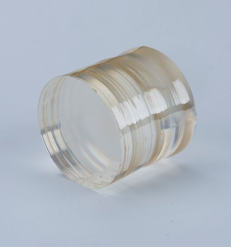
Lithium niobate, written as LiNbO3, is a synthetic ferroelectric crystal. A wafer is a thin, polished slice of this crystal prepared for device fabrication. The wafer may be coated with a metal layer, bonded to another substrate, or processed into waveguides, resonators, modulators, and sensors.
In the photonics industry, several terms are important:
Lithium niobate has a wide optical transmission range, strong second-order nonlinear susceptibility, and a large Pockels effect. The Pockels effect changes the refractive index in proportion to an applied electric field. This allows an electrical signal to control an optical signal without relying on thermal heating.
Material data help engineers compare lithium niobate with silicon, indium phosphide, gallium arsenide, and quartz. Exact values depend on wavelength, temperature, crystal composition, and measurement method, but the following properties explain why LiNbO3 remains important:
| Property | Typical significance |
|---|---|
| Chemical formula | LiNbO3 |
| Crystal type | Ferroelectric, non-centrosymmetric crystal |
| Electro-optic response | Strong linear Pockels effect, useful for high-speed optical modulation |
| Nonlinear optics | Strong second-order response for second-harmonic generation, optical parametric processes, and frequency conversion |
| Curie temperature | Approximately 1,140°C, depending on composition and measurement conditions |
| Bandgap | Commonly reported in the approximate range of 3.7–4.0 eV |
| Piezoelectric behavior | Converts mechanical strain into electrical charge and electrical fields into mechanical motion |
| Transmission range | Broad transparency from the visible region into the mid-infrared, with limits set by absorption and processing quality |
The large electro-optic coefficient is one of the main reasons lithium niobate is used in telecom modulators. A properly designed device can modulate light at data rates of tens of gigabits per second and beyond. Actual performance depends on electrode geometry, optical loss, microwave loss, impedance matching, packaging, and the selected wavelength.
A lithium niobate wafer does not operate as a complete device by itself. It becomes useful after engineers form an optical path and an electrical or mechanical control structure on the surface.
In an electro-optic modulator, an electrode applies an electric field across a waveguide. The field changes the refractive index of lithium niobate. This changes the phase or intensity of light traveling through the waveguide.
Mach–Zehnder modulators use two optical paths. When the electrical signal changes the phase difference between the paths, the output light becomes stronger or weaker. This method is widely used in fiber-optic transmitters, coherent communication, microwave photonics, and optical signal processing.
Lithium niobate can mix optical waves through its second-order nonlinear response. For example, a pump wavelength can be converted into a shorter wavelength through second-harmonic generation. Periodic poling adjusts the sign of the nonlinear coefficient along the propagation direction. This creates quasi-phase matching and improves conversion efficiency.
Engineers choosing periodically poled lithium niobate wafers for nonlinear optics must check the poling period, duty cycle, domain uniformity, crystal cut, operating wavelength, and temperature-control requirements.
Because lithium niobate is piezoelectric, an alternating voltage can create acoustic waves. This property supports surface acoustic wave filters, resonators, delay lines, and acousto-optic devices. The frequency response depends on the electrode pitch, crystal orientation, acoustic mode, and wafer thickness.
Lithium niobate modulators convert electrical data into optical signals for long-distance fiber networks. They are used in coherent transmitters, data-center interconnects, cable systems, and high-capacity optical links.
The main engineering targets are:
Microwave photonic systems use light to transport, filter, delay, or process radio-frequency signals. Lithium niobate is useful because its electro-optic response is fast and can operate across a broad frequency range. Applications include radar links, antenna remoting, satellite communication, and low-noise signal distribution.
Nonlinear lithium niobate devices can generate correlated and entangled photon pairs. Thin-film lithium niobate also supports compact waveguides, resonators, and frequency converters for quantum communication and photonic quantum information systems.
Periodically poled lithium niobate is used to convert infrared laser light into visible or other target wavelengths. This technology supports laser displays, spectroscopy, microscopy, biomedical instruments, and optical measurement equipment.
Lithium niobate can be integrated with waveguides, electrodes, and resonators to detect changes in pressure, temperature, electric field, acoustic waves, or chemical conditions. The sensor design determines whether the response comes mainly from refractive-index change, piezoelectric strain, resonance shift, or surface interaction.
Surface acoustic wave components use patterned electrodes to launch and detect mechanical waves on the wafer surface. Lithium niobate offers strong electromechanical coupling, which can support compact filters and resonators for wireless and radio-frequency systems.
Bulk lithium niobate wafers are made from a thicker crystal slice. They are well suited to traditional modulators, acoustic devices, optical windows, and applications that need a larger active volume.
Thin-film lithium niobate wafers use a thin LiNbO3 layer on a carrier substrate. The thin film confines light more strongly than a simple bulk slab. This can reduce device size and support tighter bends, dense photonic circuits, and integration with silicon photonics.
| Feature | Bulk wafer | Thin-film wafer |
|---|---|---|
| Typical structure | Single thick LiNbO3 substrate | Thin LiNbO3 layer bonded to a carrier |
| Optical confinement | Usually lower without additional waveguide processing | High when the film and cladding are properly designed |
| Integration density | Moderate | High potential |
| Processing concerns | Surface polishing, cutting, and electrode fabrication | Bond quality, film thickness, etch damage, wafer bow, and interface defects |
| Common uses | Traditional modulators, SAW devices, windows, and frequency converters | Integrated photonics, compact modulators, resonators, and quantum circuits |
When deciding how to choose lithium niobate wafers for photonics, begin with the device design rather than the wafer price. The wrong orientation or surface specification can increase fabrication time and reduce final yield.
Choose Z-cut, X-cut, or Y-cut according to the required electric-field direction, optical polarization, waveguide geometry, and electrode position. For example, many thin-film photonic platforms use X-cut or Z-cut structures to access specific electro-optic coefficients.
Common wafer diameters include 2 inches, 3 inches, 4 inches, and larger formats, although availability varies by supplier and material platform. Thickness affects mechanical strength, acoustic behavior, optical modes, and compatibility with the processing line.
Ask for measurable values rather than general descriptions such as “excellent polish.” Important specifications include:
For optical devices, request absorption data at the operating wavelength. Also check inclusions, bubbles, striations, photorefractive damage sensitivity, and crystal uniformity. A wafer that passes visual inspection may still produce high optical loss if subsurface damage or local defects are present.
Thin-film wafers may use silicon, silicon dioxide, sapphire, or another carrier. The carrier affects thermal expansion, optical confinement, electrical isolation, and compatibility with deposition and etching processes.
A useful certificate of analysis should identify the crystal composition, cut, diameter, thickness, roughness, flatness, coating status, inspection method, and batch number. For research and production work, batch traceability is important because it allows process results to be compared over time.
Although the exact process depends on the supplier, the main manufacturing steps are usually as follows:
Thin-film lithium niobate production can involve ion implantation, wafer bonding, layer transfer, annealing, and surface finishing. Etching must be carefully controlled because rough sidewalls increase scattering loss and can reduce the quality factor of resonators.
High loss may come from waveguide sidewall roughness, contamination, poor mode matching, crystal defects, or an unsuitable cladding design. Inspect the etched profile, measure propagation loss with a cutback method, and verify fiber-to-chip alignment.
Output drift can result from photorefractive damage, temperature changes, laser intensity, or packaging stress. Possible solutions include temperature control, suitable operating wavelengths, lower optical intensity, improved crystal selection, and photorefractive-resistant material grades.
Bandwidth is not determined by the wafer alone. Check electrode resistance, microwave loss, impedance matching, optical group velocity, microwave phase velocity, and package parasitics. A traveling-wave electrode can improve performance when the electrical and optical waves remain synchronized over the active length.
Use rounded wafer edges, controlled vacuum handling, soft carriers, and clean storage boxes. Avoid direct contact with polished surfaces. Thermal shocks should also be limited, particularly for bonded thin-film structures.
For periodically poled material, verify the poling period and domain quality with the supplier. Nonuniform domains can reduce conversion efficiency and create unwanted spectral peaks.
Store lithium niobate wafers in a clean, dry wafer box. Keep the polished surface away from foam, paper, dust, and metal tools. Use nitrile gloves or approved wafer-handling tools, and avoid touching the active surface.
Before processing:
Do not assume that a general glass-cleaning method is safe for every lithium niobate platform. Thin-film wafers, metal-coated wafers, and bonded wafers may require different chemical and thermal limits.
Yes. Lithium niobate is widely used for phase and intensity modulators in fiber-optic communication. Its electro-optic response supports high-speed data transmission, while the device design determines bandwidth, drive voltage, and optical loss.
Both are ferroelectric crystals with electro-optic and piezoelectric properties. Lithium niobate generally offers a stronger nonlinear optical response and is widely used for modulators and frequency conversion. Lithium tantalate may provide different thermal, acoustic, and optical performance. The correct choice depends on wavelength, temperature range, acoustic mode, and device structure.
Lithium niobate is not normally selected as a water-absorbing material. If the goal is moisture control, silica gel, molecular sieves, activated alumina, calcium chloride, or superabsorbent polymers may be more suitable, depending on the required capacity and environment. The photonic function of a lithium niobate wafer should not be confused with moisture absorption.
There is no single best cut for every modulator. X-cut and Z-cut wafers are common in integrated photonics, but the preferred option depends on the active electro-optic coefficient, optical polarization, waveguide direction, and electrode field.
Yes. Thin-film lithium niobate can be bonded to silicon or silicon dioxide platforms. This approach combines lithium niobate’s electro-optic properties with the compact routing and manufacturing infrastructure of silicon photonics.
Request the material composition, crystal cut, wafer diameter, thickness, TTV, bow, warp, surface roughness, scratch and dig rating, optical absorption, defect inspection data, coating or bonding details, and certificate of analysis. For production, also request batch traceability and sample-wafer data.
They are harder than many common glasses, but thin wafers and polished edges can still chip or crack. Correct edge treatment, clean handling, controlled clamping, and gradual temperature changes reduce the risk.
Lithium niobate combines several functions in one material: electrical control of light, frequency conversion, mechanical wave generation, and optical sensing. That combination reduces the need to use separate materials for every part of a photonic system. Thin-film processing is also improving integration density, enabling smaller modulators, resonators, sensors, and quantum photonic circuits.
The best choice depends on the final device, not on a general material ranking. Define the operating wavelength, optical mode, electrical bandwidth, wafer cut, film thickness, surface quality, and packaging method before placing an order.
Start by writing a short technical specification that includes wafer size, crystal cut, thickness, composition, optical wavelength, surface roughness, flatness, coating needs, and intended process steps. Then compare certificates of analysis, sample quality, lead time, and technical support.
For engineers developing modulators, nonlinear optical devices, acoustic filters, or integrated photonic circuits, contact CQT to discuss suitable lithium niobate wafer grades and customization options. Before fabrication, read the supplier’s user guide for cleaning, bonding, etching, storage, and handling. This preparation can reduce wafer damage, improve process repeatability, and help match the substrate to the target device.


Copyright © Hangzhou Freqcontrol
Electronic Technology Ltd.
All Rights Reserved | Sitemap |
Powered by 







 中文
中文


