The semiconductor industry relies on extreme precision. As integrated circuits become smaller, faster, and more complex, every component used in semiconductor manufacturing equipment must meet stringent requirements for purity, dimensional stability, and environmental resistance.
Among the materials widely adopted in semiconductor processing systems, quartz glass substrates have become indispensable due to their exceptional optical, thermal, and chemical properties. From photolithography systems to wafer inspection tools, quartz glass plays a critical role in maintaining process accuracy and production efficiency.
This article explores how quartz glass substrates perform in semiconductor processing equipment, their key advantages, applications, and factors buyers should consider when selecting the right material.
Quartz glass substrates, also known as fused silica substrates, are high-purity silicon dioxide (SiO₂) materials manufactured through advanced melting or flame deposition processes.
Unlike crystalline quartz, quartz glass has an amorphous structure that provides superior uniformity and stability.
Common semiconductor-grade quartz materials include:
Synthetic fused silica
High-purity quartz glass
UV-grade fused silica
HPFS (High Purity Fused Silica)
Corning 7980 fused silica
JGS1 optical quartz
These materials are engineered to withstand the demanding conditions found in semiconductor fabrication facilities.
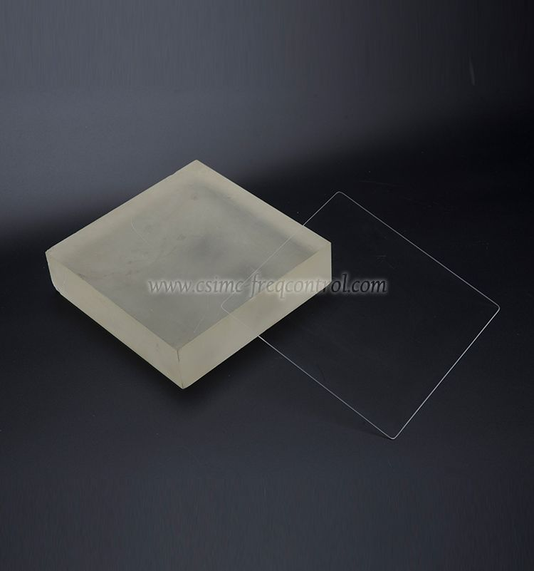
Semiconductor fabrication environments expose materials to:
High temperatures
Intense UV radiation
Plasma processing
Aggressive chemicals
Extreme cleanliness requirements
Precision alignment systems
Quartz glass substrates excel because they can maintain their performance without contamination or deformation.
Their unique combination of properties makes them one of the most trusted materials in semiconductor equipment manufacturing.
1. Exceptional Thermal Stability
Semiconductor processes often involve rapid temperature fluctuations.
Quartz glass has an extremely low coefficient of thermal expansion, allowing it to maintain dimensional stability even under severe thermal cycling conditions.
Benefits:
Minimal thermal deformation
Excellent thermal shock resistance
Stable performance at elevated temperatures
Improved process consistency
This is particularly important in diffusion furnaces and deposition equipment.
2. Ultra-High Purity Reduces Contamination Risks
Modern semiconductor devices are manufactured at nanometer scales, where microscopic contamination can significantly impact yield.
High-purity quartz glass contains extremely low levels of impurities, reducing particle generation and contamination risks.
Advantages include:
Reduced defect rates
Improved wafer yields
Cleaner manufacturing environments
Better long-term equipment reliability
Purity is one of the primary reasons synthetic fused silica is preferred over conventional glass materials.
3. Excellent UV and Optical Transmission
Photolithography systems rely heavily on ultraviolet light to transfer circuit patterns onto silicon wafers.
Quartz glass offers outstanding transmission across a broad wavelength range.
Typical transmission range:
UV: 180 nm – 400 nm
Visible: 400 nm – 700 nm
Near-infrared: up to 2500 nm
Benefits:
Improved pattern accuracy
Enhanced optical system efficiency
Lower energy losses
Better imaging precision
Advanced lithography equipment frequently utilizes ArF and KrF-grade fused silica.
4. Superior Chemical Resistance
Semiconductor fabrication involves exposure to aggressive chemicals such as:
Acids
Solvents
Reactive gases
Cleaning agents
Quartz glass demonstrates exceptional chemical durability.
Benefits include:
Corrosion resistance
Longer service life
Reduced maintenance costs
Consistent performance
This durability makes it suitable for harsh production environments.
5. Excellent Plasma Resistance
Many semiconductor processes utilize plasma etching.
Quartz glass maintains structural integrity during plasma exposure.
Advantages:
Reduced surface degradation
Stable process performance
Lower contamination risks
Extended component lifespan
Plasma resistance is especially important in advanced chip manufacturing.
Photolithography Systems
Quartz glass is widely used in:
Projection optics
Photomasks
Optical windows
UV lenses
These components require exceptional optical precision and minimal distortion.
Wafer Inspection Equipment
Inspection systems demand high optical clarity.
Quartz glass components include:
Optical windows
Beam splitters
Protective covers
Precision optical elements
These systems help detect microscopic defects during production.
Semiconductor Furnaces
Quartz components are used in:
Diffusion tubes
Wafer carriers
Furnace liners
Process chambers
Their thermal stability ensures accurate temperature control.
Plasma Etching Equipment
Quartz glass supports plasma-based manufacturing processes.
Applications include:
Chamber liners
Process windows
Gas distribution components
Protective shields
Metrology Equipment
Measurement systems utilize quartz glass because of its dimensional stability.
Applications include:
Interferometers
Precision stages
Alignment systems
Optical calibration devices
Corning 7980
Features:
Ultra-high purity
Excellent optical homogeneity
Superior UV transmission
Low birefringence
Outstanding thermal stability
Applications:
Photolithography
Laser optics
Semiconductor inspection
JGS1 Quartz Glass
Features:
High UV transmission
Good thermal stability
Cost-effective solution
Applications:
Optical windows
UV systems
Standard semiconductor optics
Synthetic Fused Silica
Features:
Extremely low impurity content
Excellent optical performance
High durability
Applications:
Advanced semiconductor equipment
Precision optical systems
Purity Level
Higher purity means lower contamination risks.
Choose semiconductor-grade materials with ultra-low metal impurities.
Optical Requirements
Consider:
UV wavelength compatibility
Transmission performance
Optical homogeneity
Birefringence levels
Thermal Requirements
Evaluate:
Operating temperature
Thermal cycling frequency
Thermal shock resistance
Surface Quality
Important parameters include:
Surface roughness
Flatness
Scratch-dig specifications
Parallelism
Dimensional Tolerances
High-precision applications require strict tolerances for:
Thickness
Diameter
Flatness
Surface accuracy
As semiconductor technologies continue to evolve, quartz glass demand will grow in several areas:
Advanced Lithography
Extreme ultraviolet (EUV) systems require increasingly precise optical materials.
AI Chip Manufacturing
Artificial intelligence processors require tighter tolerances and cleaner production environments.
3D Semiconductor Packaging
Advanced packaging technologies demand highly precise optical and thermal components.
Smaller Process Nodes
As chip geometries shrink, material purity becomes even more critical.
Quartz glass will continue to be a foundational material supporting next-generation semiconductor innovation.
Quartz glass substrates have become essential materials in semiconductor processing equipment due to their unique combination of thermal stability, optical clarity, chemical resistance, and ultra-high purity.
From photolithography and plasma etching to wafer inspection and precision metrology, quartz glass enables manufacturers to achieve the accuracy, reliability, and consistency required for advanced semiconductor production.
As semiconductor technologies become more sophisticated, high-performance quartz glass materials such as synthetic fused silica and Corning 7980 will remain indispensable for enabling future innovation.



Copyright © Hangzhou Freqcontrol
Electronic Technology Ltd.
All Rights Reserved | Sitemap |
Powered by 







 中文
中文


