As 5G phones support more frequency bands, wider channels, and higher data rates, the RF front end must separate signals with greater accuracy. Lithium Niobate Wafers for 5G RF filters help manufacturers build compact acoustic filters with strong piezoelectric performance and low signal loss. They are used in SAW, temperature-compensated SAW, and thin-film acoustic devices. This article explains how lithium niobate works, where it fits in a 5G RF front-end module, how to select a wafer, and what buyers should check before placing an order.
A smartphone RF front end sits between the antenna and the transceiver. It includes filters, duplexers, multiplexers, switches, power amplifiers, and low-noise amplifiers. Its main job is to send the correct signal while blocking signals from nearby bands.
5G increases this challenge in three ways:
Without a sharp filter, a strong nearby signal can reduce receiver sensitivity or create unwanted intermodulation products. The result may be slower data transfer, dropped connections, or poor performance near a busy base station.
For this reason, RF designers look for materials that combine high electromechanical coupling, stable frequency response, low acoustic loss, and compatibility with wafer manufacturing. Lithium niobate is one of the materials that can meet these requirements.
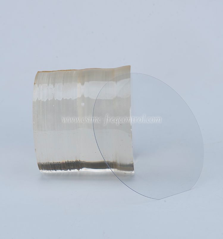
Lithium niobate wafers are polished semiconductor and photonic substrates made from lithium niobate, with the chemical formula LiNbO3. Lithium niobate is a ferroelectric crystal with strong piezoelectric, electro-optic, nonlinear optical, and acousto-optic properties.
In an RF filter, a metal electrode pattern is placed on or above the wafer. This pattern is usually called an interdigital transducer, or IDT. When an electrical signal reaches the IDT, the piezoelectric crystal converts part of the electrical energy into a mechanical acoustic wave. A second electrode converts the selected acoustic wave back into an electrical signal.
The frequency is mainly controlled by the electrode pitch and the acoustic velocity:
f ≈ v / λ
This allows engineers to create filters for specific 5G bands by adjusting crystal orientation, film thickness, electrode spacing, and device layout.
Lithium niobate can be used in several acoustic filter structures. The correct structure depends on the target frequency, bandwidth, insertion loss, temperature range, and production cost.
In a surface acoustic wave, or SAW, filter, the acoustic energy travels close to the wafer surface. The IDT launches and receives the wave. The filter response is shaped by the electrode pattern and reflector design.
Lithium niobate has a high piezoelectric response. In practical terms, this can help produce strong electrical-to-acoustic conversion and a useful filter response with a small device footprint. SAW filters are commonly considered for lower and mid-band RF applications where the required frequency and power range match the material and design.
Acoustic velocity changes with temperature. If the velocity changes, the filter center frequency also shifts. This is a concern for phones exposed to outdoor cold, direct sunlight, or heat from high-performance processors.
Temperature-compensated SAW designs use added layers or engineered structures to reduce the total temperature coefficient of frequency. The goal is not to claim that lithium niobate has no temperature drift. Instead, the device stack is designed so that the temperature effects of different materials partly offset each other.
Thin-film lithium niobate wafers for RF front-end devices use a thin lithium niobate layer bonded to or supported by another substrate. The thin film can improve acoustic confinement and support advanced resonator designs, including guided-wave and Lamb-wave structures.
Thin-film designs can offer a wider design range than a simple bulk-crystal device. Engineers can tune the lithium niobate thickness, electrode material, substrate, and acoustic mode. However, performance depends strongly on film uniformity, bonding quality, surface roughness, and process control.
A duplexer separates the transmit and receive paths in a frequency-division duplex system. A multiplexer combines several filter paths so that one antenna can support multiple bands.
In these components, the filter must provide:
Lithium niobate is not the only material used for these functions. Lithium tantalate, aluminum nitride, zinc oxide, silicon, and other engineered structures are also important. Material selection should be based on measured device data rather than on a single material label.
Piezoelectric coupling determines how effectively an electrical signal can excite an acoustic wave. Strong coupling gives designers more control over filter bandwidth and impedance.
Lithium niobate is known for its strong piezoelectric behavior. The exact result depends on crystal cut, propagation direction, electrode design, and the complete layer stack. Therefore, suppliers should provide measured parameters for the selected wafer orientation instead of offering only a general material name.
5G channels are wider than many earlier cellular channels. A filter with a narrow passband may not cover the full useful signal. A filter with a wide passband but weak rejection may allow interference into the receiver.
Lithium niobate gives engineers a wide design space for acoustic coupling. This can help balance bandwidth and selectivity. The final bandwidth must still be verified through measurements such as S-parameters, insertion loss, return loss, and rejection.
Acoustic filters operate according to the wavelength of the acoustic wave rather than the physical wavelength of the radio signal in air. This allows a filter to be much smaller than a conventional lumped or distributed RF structure at the same operating frequency.
A smaller filter helps module designers fit more RF paths into a smartphone, router, or small-cell radio. Size reduction also creates challenges, including tighter lithography limits, higher sensitivity to particles, and stronger parasitic effects from packaging.
Lithium niobate can be supplied as a bulk wafer or as a thin film on a supporting substrate. This supports different manufacturing routes, such as:
Thin-film integration is especially useful when designers need better acoustic confinement or integration with semiconductor processing. The wafer supplier must control thickness variation and bonding defects because small changes can shift the resonant frequency.
Lithium niobate is also widely used in optical modulators because of its electro-optic effect. This matters for 5G infrastructure, where optical links connect radio units, distributed units, data centers, and transport networks.
In other words, the same material family can support both wireless RF components and high-speed optical communication components. The wafer specification is not the same for both applications, but the material platform has value across the communications supply chain.
When choosing a wafer, buyers should request a complete specification sheet. “High quality” is not a measurable specification. The following data points are more useful.
| Specification | Why It Matters | What to Check |
|---|---|---|
| Wafer diameter | Determines equipment compatibility and die output. | Common sizes include 2-inch, 3-inch, 4-inch, and larger formats. |
| Crystal cut and orientation | Changes acoustic velocity, coupling, and temperature behavior. | Confirm the cut, propagation direction, and orientation mark. |
| Thickness | Controls mechanical behavior and thin-film device modes. | Review nominal thickness, tolerance, and mapping method. |
| Surface roughness | A rough surface can increase scattering and reduce process yield. | Request Ra or RMS roughness data and the measurement area. |
| Total thickness variation | Thickness variation can cause frequency variation across the wafer. | Check TTV, bow, warp, and measurement points. |
| Flatness and bow | Influences lithography focus, bonding, and chuck contact. | Review bow and warp limits for the actual process tool. |
| Defect density | Particles, pits, cracks, and inclusions reduce usable die area. | Ask for inspection rules, defect size limits, and sample reports. |
| Resistivity and conductivity | Can affect electrical loss and device isolation. | Confirm whether the application needs congruent, stoichiometric, or doped material. |
| Temperature coefficient | Frequency drift can affect filter performance over temperature. | Check wafer and device-level temperature data separately. |
Start with the intended band and device type. Record the center frequency, passband width, required rejection, maximum input power, operating temperature, and package size.
For example, a filter for a sub-6 GHz 5G handset will have different requirements from a filter for a base-station radio or a millimeter-wave module. Do not select a wafer before defining the RF target.
Choose between SAW, temperature-compensated SAW, Lamb-wave, or another resonator structure. The mode determines the suitable wafer thickness, orientation, electrode material, and support substrate.
A wafer that performs well in an optical modulator may not be the correct choice for a high-volume acoustic filter. Application-specific engineering is essential.
Check whether the wafer works with the available cleaning, lithography, deposition, etching, bonding, and dicing processes. Important questions include:
Do not approve a supplier from a brochure alone. Run a sample evaluation using the same process conditions planned for production.
Measure wafer-level and device-level results, including:
Ask for a certificate of analysis, lot traceability, inspection records, packaging details, and change-control procedures. For high-volume RF production, a stable supply is as important as a strong first sample.
Also confirm lead time, minimum order quantity, sample policy, export documents, and technical support. These details can affect the total development schedule more than the initial wafer price.
Local thickness variation, crystal non-uniformity, electrode dimensions, and temperature gradients can cause frequency variation. A wafer map can show whether the problem is random or follows a location pattern.
Scratches, pits, edge chips, and particles can cause open circuits, shorts, acoustic scattering, or bonding failure. Optical inspection alone may not detect every defect that matters to the final device.
Lithium niobate does not eliminate thermal frequency shift. If the product operates across a wide temperature range, the design may require a compensation layer, a controlled package, or electronic calibration.
A good wafer can still produce a poor RF module if the package adds parasitic capacitance, unwanted acoustic loss, or poor thermal control. Test the complete device, not only the bare die.
Lithium niobate is often described as a high-performance material, but no wafer is ideal for every RF design. High power, low loss, thermal stability, frequency range, cost, and production yield must be considered together.
| Advantages | Limitations to Manage |
|---|---|
| Strong piezoelectric response | Performance depends on crystal cut and device structure |
| Suitable for compact acoustic filters | Surface defects can reduce yield |
| Supports SAW and thin-film designs | Thin-film bonding adds process complexity |
| Useful for wideband filter engineering | Temperature compensation may still be required |
| Available in different wafer sizes and orientations | Cost and supply depend on grade, diameter, and tolerance |
| Also used in optical communication components | RF and photonic specifications are not interchangeable |
The following sources can help engineers verify 5G and material requirements:
These references do not replace product qualification. A wafer must still be tested in the customer’s own process and RF design.
When a project requires a lithium niobate wafer supplier for 5G applications, CQT can be included in the technical comparison process. Buyers should ask CQT or any potential supplier for the exact wafer cut, diameter, thickness tolerance, TTV, bow, warp, surface roughness, defect limits, packaging method, and lot traceability.
A useful supplier evaluation should include:
Contact CQT with the target frequency, device structure, wafer size, thickness, crystal orientation, and manufacturing process. These details allow the supplier to recommend a more suitable wafer instead of offering a generic material grade.
No. 5G RF filters can use lithium niobate, lithium tantalate, aluminum nitride, zinc oxide, silicon, and other material systems. The selection depends on frequency, bandwidth, power handling, temperature stability, size, cost, and manufacturing yield.
Bulk lithium niobate is a thicker crystal wafer. Thin-film lithium niobate uses a thin active layer on a supporting substrate. Thin-film structures can provide stronger acoustic confinement and more design flexibility, while bulk wafers may offer a simpler process for certain device types.
No. Insertion loss depends on the complete filter design. Electrode resistance, acoustic scattering, surface roughness, substrate loss, packaging, impedance matching, and temperature all affect the measured result.
There is no universal best cut. The correct orientation depends on the acoustic mode and target frequency. The supplier and device designer should select the cut together and confirm it through wafer and device testing.
Choose a diameter that matches the fabrication line and the expected die output. A larger wafer may reduce cost per die, but only if the equipment, handling system, yield, and supplier capacity support it.
Store polished wafers in clean, protective containers under the supplier’s recommended temperature and humidity conditions. Avoid direct contact with the polished surface. Follow the agreed cleaning and unpacking procedure before processing.
Yes. Lithium niobate is widely used in electro-optic and photonic components, including high-speed optical modulators. However, optical wafers require different specifications, such as optical loss, film uniformity, domain control, and electrode design.
Lithium niobate wafers are widely considered for 5G RF front-end devices because they combine strong piezoelectric behavior, compact acoustic filter design, and compatibility with bulk and thin-film structures. Their value is clearest when the wafer cut, thickness, surface quality, acoustic mode, and temperature design are matched to a specific RF target.
The next step is to prepare a wafer requirement sheet and request a sample evaluation. Include the frequency band, filter type, wafer diameter, crystal orientation, thickness tolerance, surface roughness, TTV, bow, warp, and quality documentation. For a project that needs a reliable lithium niobate wafer supplier for 5G applications, discuss the specifications and trial plan with CQT before moving to volume production.


Copyright © Hangzhou Freqcontrol
Electronic Technology Ltd.
All Rights Reserved | Sitemap |
Powered by 







 中文


