Modern semiconductor, photonics, and thin-film equipment needs a support material that remains stable under heat, chemicals, and ultraviolet light. A high purity Quartz Glass Substrate for semiconductor processing provides low thermal expansion, high optical transmission, and strong chemical resistance in one platform. It is used in wafer handling, optical coating, sensors, LEDs, laboratory devices, and deposition systems. This guide explains what a quartz glass substrate is, how it compares with sapphire and fused silica, how to select the correct grade, and how to avoid common processing failures.
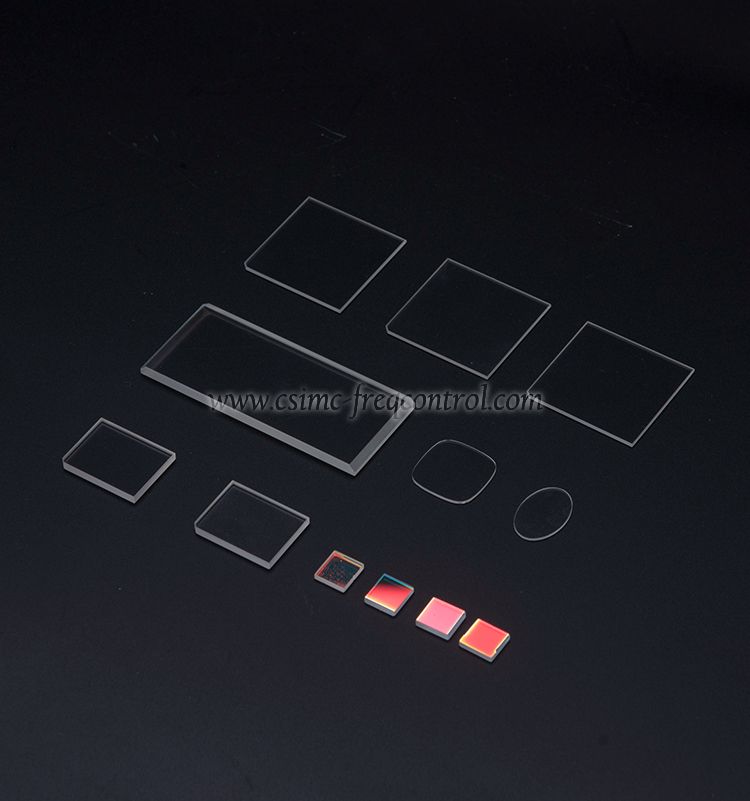
A quartz glass substrate is a flat plate, wafer, disc, or custom part made from high-purity silicon dioxide, written as SiO2. In industry, the terms quartz glass, fused quartz, and fused silica are often used for materials with the same basic chemical composition. The main difference is usually the raw material and manufacturing route:
Unlike ordinary glass, quartz glass has an amorphous, non-crystalline structure. It does not have the regular crystal lattice found in sapphire. This structure helps it maintain dimensional stability during repeated heating and cooling.
| Term | Meaning | Why it matters |
|---|---|---|
| Purity | The amount of SiO2 and the level of trace metals or other contaminants | Low contamination is important for semiconductor and optical coating processes |
| CTE | Coefficient of thermal expansion, measured in ppm/°C | A low CTE reduces dimensional change during temperature cycling |
| Surface roughness | The small-scale height variation on a polished surface, often measured as Ra | Lower roughness improves coating uniformity and optical performance |
| Transmission range | The wavelength range in which the material allows light to pass | It determines whether the substrate is suitable for UV, visible, or infrared systems |
| OH content | The concentration of hydroxyl groups in the glass | It can affect infrared absorption and high-temperature behavior |
Material performance changes with grade, production method, thickness, surface finish, and measurement conditions. The values below are typical engineering ranges rather than a guarantee for every product.
| Property | Typical quartz glass value | Design meaning |
|---|---|---|
| Composition | Approximately 99.9% to 99.999% SiO2, depending on grade | Higher purity reduces unwanted ionic and metallic contamination |
| Density | Approximately 2.2 g/cm³ | Useful when calculating stage load and handling weight |
| Thermal expansion | About 0.5 ppm/°C near room temperature for many fused silica grades | Much smaller dimensional change than common borosilicate or soda-lime glass |
| Softening point | Approximately 1,600°C to 1,720°C, depending on grade and test method | Suitable for many high-temperature process environments |
| Visible transmission | Often above 90% for polished, suitable-thickness parts, excluding reflection losses | Supports optical inspection and photonics applications |
| Electrical resistivity | Very high at room temperature; the exact value depends on temperature and grade | Useful for electrical insulation and dielectric structures |
For reference, the National Institute of Standards and Technology provides technical data for fused silica and other optical materials. Corning also publishes fused silica product information, including optical and thermal characteristics. Heraeus supplies high-purity fused silica for semiconductor, lamp, optical, and laboratory applications. Always compare the supplier’s certificate of analysis with your process limits before approving a batch.
Quartz glass and fused silica are often chemically similar, so the real comparison may be between different grades and manufacturing routes. Sapphire is different: it is single-crystal aluminum oxide, or Al2O3. The best material depends on temperature, load, optical wavelength, hardness, contamination limits, and budget.
| Feature | Quartz glass | Fused silica | Sapphire |
|---|---|---|---|
| Main composition | SiO2 | SiO2 | Al2O3 |
| Structure | Amorphous | Amorphous | Single crystal |
| Thermal expansion | Very low, commonly around 0.5 ppm/°C | Very low, grade dependent | Higher than fused silica, commonly around 5 to 8 ppm/°C |
| Hardness | Lower than sapphire | Lower than sapphire | Mohs hardness of about 9 |
| Thermal shock resistance | Strong because of its low CTE | Strong because of its low CTE | Good, but thermal stress must be checked during rapid cycling |
| UV performance | Depends on purity and OH level | Often selected for deep-UV optical work | Useful in selected UV, visible, and infrared ranges |
| Typical cost position | Often lower than sapphire for simple flat parts | Varies by synthetic purity and finish | Often higher because of crystal growth and machining |
Choose quartz glass or fused silica when low thermal expansion, chemical resistance, optical transmission, and electrical insulation are the main requirements. Choose sapphire when scratch resistance, mechanical hardness, or a single-crystal surface is more important. For a process involving strong plasma, high particle control, or deep-UV exposure, ask for data specific to wavelength, plasma chemistry, and surface treatment rather than relying on a general material name.
Quartz glass substrates and quartz components are used in wafer carriers, process boats, thermal processing fixtures, inspection windows, and deposition systems. The material’s low thermal expansion helps reduce dimensional movement during furnace cycles. Its low metal content can also help reduce contamination risk when a high-purity grade is properly cleaned and handled.
Typical process areas include:
A quartz glass substrate for photonics and semiconductor wafers can be used for optical filters, beam splitters, windows, mirrors, UV components, and sensor covers. The substrate is usually polished to control flatness, parallelism, scratch-dig quality, and surface roughness. Optical designers should specify the wavelength range because transmission is not identical from ultraviolet to infrared.
Quartz substrates and carriers may support epitaxy, thin-film deposition, annealing, and inspection. The correct choice depends on the process temperature, the required thermal uniformity, and whether the substrate directly contacts the product wafer.
Quartz glass is suitable for optical observation, chemical exposure, and high-temperature laboratory systems. It can be combined with metal films, transparent conductive layers, or patterned coatings. Before use, confirm that the cleaning chemistry will not attack the coating or create surface residues.
Flat quartz glass parts can be used as deposition supports, furnace components, and optical covers. For thin-film work, surface cleanliness and roughness are important because particles or polishing residue can create pinholes and non-uniform film thickness.
The substrate is not just a passive plate. It affects temperature uniformity, film adhesion, particle levels, optical loss, alignment, and product yield.
Record the highest and lowest temperatures, heating rate, cooling rate, vacuum level, gas type, plasma exposure, and chemical contact. A part that performs well in a dry furnace may not perform the same way in wet etching or plasma cleaning.
Ask the supplier for a trace-element specification or certificate of analysis. Semiconductor processes may require control of sodium, potassium, iron, aluminum, calcium, and other metallic impurities. Do not select “high purity” from a marketing description alone; request actual limits in parts per million or parts per billion when required.
Important dimensions include:
Thin substrates may reduce weight but can bend during heating, vacuum loading, or coating. A thicker substrate may improve stiffness but increase thermal mass and cost.
Define surface roughness, scratch-dig quality, polishing method, and allowable chips. A rough surface may improve mechanical bonding in some designs, while a polished surface is usually preferred for optical transmission, thin films, and particle-sensitive equipment.
State the working wavelength, angle of incidence, required transmission, allowable scatter, and whether an anti-reflection coating is needed. UV applications may require synthetic fused silica with controlled absorption rather than a general-purpose quartz grade.
Request a cleaning method that matches the process. The supplier should explain whether the part is shipped in a clean bag, double bag, vacuum package, or other controlled packaging. Even a low-contamination substrate can be compromised by fingerprints, fibers, polishing slurry, or unsuitable storage.
Machining quartz glass requires careful control because the material is hard but brittle. Excessive point loading can cause edge chipping or subsurface damage. A qualified supplier should control tool wear, coolant cleanliness, polishing pressure, and inspection lighting.
| Problem | Likely cause | Practical solution |
|---|---|---|
| Cracks after heating | Thermal shock, edge damage, or residual stress | Use proper annealing, improve edge finishing, and reduce heating or cooling rate |
| Film peeling | Organic residue, particles, unsuitable roughness, or poor surface activation | Review cleaning, surface energy, deposition temperature, and coating compatibility |
| High particle count | Inadequate cleaning, packaging dust, or contact with worn equipment | Use controlled cleaning, clean packaging, gloves, and particle inspection |
| Optical haze | Micro-scratches, subsurface damage, contamination, or incorrect grade | Check polishing quality and measure transmission at the working wavelength |
| Dimensional drift | Temperature variation, poor support, or incorrect CTE assumption | Model thermal expansion and support the substrate evenly |
| Chemical attack | Exposure to hydrofluoric acid or strong hot alkali | Confirm chemical compatibility or select another material |
Handle quartz glass with powder-free gloves and hold it by the edges whenever possible. Avoid metal tweezers on polished areas because they can create scratches and particles. Store substrates vertically or in a designed carrier if the geometry allows it. Do not place a clean substrate on an unverified bench surface.
For cleaning, use a validated process rather than a universal recipe. A typical workflow may include solvent cleaning, ultrapure water rinsing, filtered drying, and inspection. The exact chemical sequence depends on the coating, contamination type, and equipment. Hydrofluoric acid can etch quartz glass and should only be used under an approved chemical safety procedure.
Before placing a production order, ask for the following information:
CQT can be included in the supplier comparison when you need custom quartz glass parts, substrate processing, or technical support. Share your drawing, process temperature, chemicals, wavelength, purity target, and inspection standard. A supplier can then recommend a grade based on measurable requirements instead of a general product label.
They are both mainly amorphous SiO2, but the terms can describe different raw materials and production methods. Ask for the exact grade, impurity limits, OH content, and optical data before treating them as interchangeable.
Many quartz glass grades can operate at 1,000°C, but the result depends on load, atmosphere, heating rate, geometry, and exposure time. The softening point is not the same as a recommended continuous-use temperature. Obtain a supplier’s temperature recommendation for the exact design.
Sapphire is much harder and more scratch-resistant. Quartz glass usually offers lower thermal expansion and strong thermal shock resistance. “Stronger” should therefore be divided into hardness, fracture toughness, thermal shock resistance, and load-bearing capability.
No general approval should be assumed. Hydrofluoric acid attacks silica, so quartz glass may be etched or damaged. Confirm the chemical process with a materials specialist and follow the required safety controls.
There is no single correct value. Optical parts, thin-film substrates, and bonding surfaces have different requirements. Specify Ra or another measurement method, together with flatness, scratch-dig quality, and the working wavelength when applicable.
Improve edge finishing, reduce point contact, use a compatible carrier, control heating and cooling rates, and inspect for chips before processing. Packaging and operator handling are also common sources of damage.
Start with a process specification rather than a material name. Record temperature, chemistry, wavelength, purity, dimensions, flatness, roughness, and cleaning requirements. Then compare a sample against your actual process and inspect it for particles, cracks, optical loss, film adhesion, and dimensional change. For a custom quartz glass substrate supplier for thin film deposition, contact CQT with your drawing and test conditions, review the technical datasheet, and request a sample or user guide before moving to volume production.


Copyright © Hangzhou Freqcontrol
Electronic Technology Ltd.
All Rights Reserved | Sitemap |
Powered by 







 中文


