Typical Applications Driving Demand for High-Purity Quartz Wafers include semiconductor processing, MEMS fabrication, optical communications, RF frequency control, photonics, sensor development, and laboratory research. A high-purity quartz wafer is a thin, precision-machined disc or substrate made from low-contamination quartz, such as fused silica or single-crystal quartz. Its value is practical: it provides thermal stability, chemical resistance, electrical insulation, and low impurity levels in processes where contamination or dimensional instability can reduce product yield.
For manufacturers, selecting the right Single Crystal Quartz Wafers can improve process repeatability, protect sensitive devices from metallic contamination, and reduce unplanned downtime. For buyers working with CQT or another qualified supplier, the specification should cover quartz grade, crystal orientation, diameter, thickness, surface finish, flatness, parallelism, edge profile, cleaning, packaging, and inspection documentation.
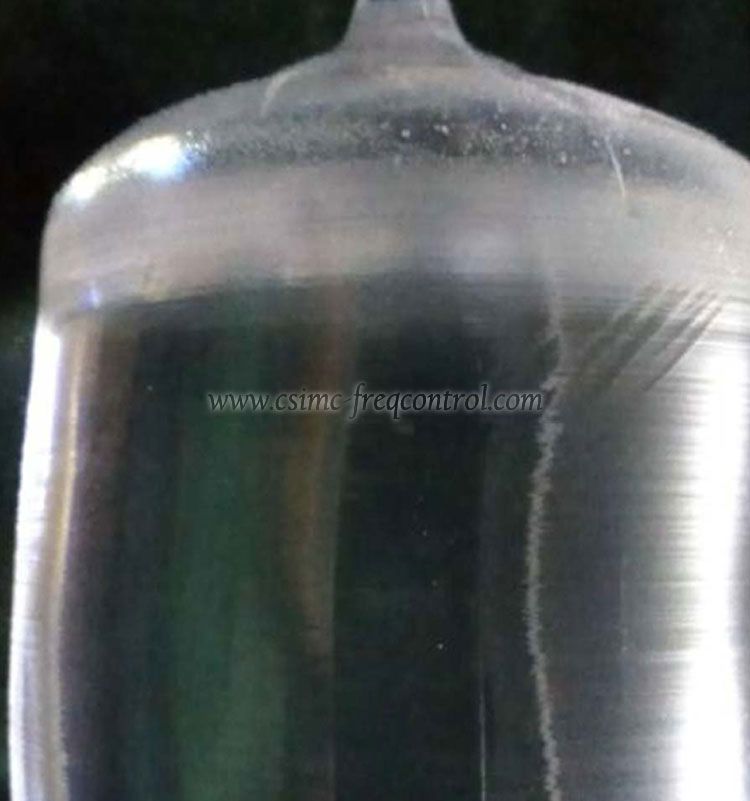
High-purity quartz wafers are engineered substrates manufactured to control trace elements, particles, surface defects, and geometry. Depending on the application, the material may be:
The term “high purity” does not describe one universal grade. In semiconductor and photonics manufacturing, buyers often define allowable metallic impurities, alkali contamination, hydroxyl content, inclusions, bubbles, and surface particles in a controlled material specification. A supplier should therefore provide a certificate of conformity, lot traceability, and inspection results rather than relying only on a general “high-purity” label.
The demand is closely connected to the miniaturization and higher operating performance of modern electronics. As device features become smaller and process windows become narrower, even small particles, out-of-flatness, or thermal distortion can affect yield.
Quartz is attractive because it combines several properties that are difficult to obtain in one substrate:
Historically, quartz was used in laboratory glassware, optical components, and piezoelectric resonators. As semiconductor manufacturing, surface acoustic wave technology, and precision photonics developed, quartz evolved from a general-purpose material into a tightly specified process component. This industrial shift explains why Typical Applications Driving Demand for High-Purity Quartz Wafers now extend beyond traditional laboratory use.
Semiconductor fabs use quartz components in wafer handling, diffusion, oxidation, chemical vapor deposition, plasma processing, and cleaning systems. Quartz wafers can function as carrier substrates, process monitors, calibration substrates, or specialized components in high-temperature environments.
In compound-semiconductor manufacturing, including gallium nitride, silicon carbide, gallium arsenide, and related technologies, a quartz substrate may be selected for:
Here, surface particles and trace metals are not cosmetic issues. They can create nucleation defects, alter film uniformity, or reduce device yield. This is why a buyer should request documented cleaning procedures, particle inspection, and packaging controls from CQT or another approved source.
MEMS manufacturers use quartz substrates for microfluidic devices, resonators, pressure sensors, inertial sensors, and laboratory-on-chip structures. Quartz is especially useful when the design requires electrical insulation, optical transparency, chemical resistance, or stable behavior during wet etching and bonding.
For MEMS production, the critical parameters may include:
These details directly affect lithography focus, bonding yield, resonant frequency, and alignment accuracy. Therefore, Single Crystal Quartz Wafers should be ordered against a controlled drawing rather than a diameter-only description.
Single-crystal quartz is a core material for crystal oscillators, resonators, filters, and timing modules. Its piezoelectric response allows mechanical vibration to be converted into a stable electrical frequency. AT-cut and related crystal orientations are selected for their temperature-frequency characteristics and frequency stability.
In RF frequency-control production, wafer quality influences:
CQT buyers should define crystallographic orientation, thickness tolerance, surface condition, electrode compatibility, and frequency-related requirements at the quotation stage. A dimensional tolerance such as ±0.01 mm may be appropriate for some machined features, but it should never be assumed to represent the complete wafer specification.
Quartz wafers and quartz substrates are used in optical windows, photonic structures, UV components, sensor platforms, and thin-film deposition processes. Fused silica is often preferred where amorphous structure, low optical absorption, and broad transmission are important.
Typical optical requirements include:
It is a common mistake to treat every quartz wafer as an optical-grade wafer. Optical performance depends on material type, wavelength, thickness, surface polish, coatings, and inspection method. The end-use wavelength must be stated clearly before selecting a material.
Research laboratories and advanced manufacturing lines use high-purity quartz wafers as substrates for thin-film deposition, annealing, sputtering, atomic layer deposition, and chemical vapor deposition. The substrate must remain stable while researchers evaluate film thickness, stress, crystallinity, conductivity, and optical response.
Quartz is valuable in these applications because it contributes less background conductivity than many metal-containing materials and can tolerate repeated thermal exposure. However, repeated furnace cycles may still produce surface deposits, devitrification, or dimensional changes. A preventive maintenance plan and post-process inspection are therefore essential.
Quartz wafers are also used in biosensors, electrochemical platforms, microreactors, and analytical instruments. Their chemical resistance and optical transparency support fluorescence detection, spectroscopy, and surface-functionalization research.
For these applications, buyers should confirm:
Although application demand is expanding, procurement errors remain common. The following table provides a practical starting point for a CQT technical inquiry.
| Specification | Why It Matters | Typical Verification Approach |
|---|---|---|
| Quartz type | Determines thermal, optical, electrical, and piezoelectric behavior. | Material certificate, Raman or optical examination where required. |
| Purity and trace metals | Controls contamination risk in semiconductor and analytical processes. | Supplier CoC, ICP-MS or customer-approved chemical analysis. |
| Diameter and thickness | Ensures compatibility with holders, chucks, and process tools. | Calibrated dimensional measurement; tolerance may reach 0.01 mm for defined features. |
| Flatness, TTV, bow, and warp | Supports lithography, bonding, alignment, and uniform deposition. | Optical flatness measurement, profilometry, or customer-approved metrology. |
| Surface roughness | Affects adhesion, friction, optical scattering, and device performance. | AFM, white-light interferometry, or stylus profilometry. |
| Particles and visual defects | Reduces yield loss and process contamination. | 100% visual inspection plus particle inspection when specified. |
For material references, ASTM E438 is commonly associated with laboratory glass and glass material classifications, while customer semiconductor specifications may use SEMI documents or internal fab standards. Because no single standard covers every quartz wafer application, the purchase order should identify the exact test method, acceptance limit, sampling plan, and reporting format. DIN-based dimensional or surface specifications may also be used when required by the customer’s engineering documentation.
They are related but not identical. Fused silica is amorphous, while Single Crystal Quartz Wafers have an ordered crystalline structure and a defined orientation. Their thermal expansion, optical response, piezoelectric behavior, and processing characteristics can differ significantly.
Purity is important, but it is only one part of performance. A wafer with excellent chemical purity may still fail if its flatness, roughness, thickness uniformity, edge quality, or crystal orientation is unsuitable for the process.
“Polished” does not define roughness, waviness, particles, metallic residues, or total thickness variation. Buyers should request measurable limits and inspection records, including 100% inspection when the application has a low defect tolerance.
Quartz has strong thermal resistance, but contamination, devitrification, mechanical stress, rapid temperature changes, and process deposits can shorten service life. The actual furnace profile and cleaning chemistry should be included in qualification testing.
Diameter alone is not enough. Notch or flat orientation, edge bevel, thickness, chuck compatibility, handling method, and wafer identification may all affect tool integration.
Consider an RF component manufacturer developing a new crystal resonator. The initial request is for “high-purity quartz wafers,” but that description is too broad for production control. A stronger technical specification would identify:
With those requirements defined, CQT can evaluate whether the material should be supplied as a standard catalog item or manufactured as a custom quartz wafer. The result is a more reliable comparison between suppliers, fewer engineering changes, and a clearer path from prototype qualification to volume production.
When the application is safety-critical, yield-sensitive, or difficult to reproduce, buyers should use a staged qualification process:
For responsive technical sourcing, a buyer may request a quotation acknowledgment within 24 hours, but response time should not replace engineering review. The most trustworthy supplier is one that clearly distinguishes guaranteed specifications from achievable targets and explains how each parameter is measured.
The continued expansion of semiconductor devices, RF modules, optical sensors, MEMS products, and advanced research tools is sustaining demand for both fused-silica substrates and Single Crystal Quartz Wafers. Their value comes from a combination of purity, dimensional stability, chemical resistance, optical performance, and—in crystalline forms—piezoelectric behavior.
The central lesson behind Typical Applications Driving Demand for High-Purity Quartz Wafers is that application requirements must determine material selection. A wafer for a UV optical platform is not specified in the same way as a wafer for an RF resonator, semiconductor furnace, or microfluidic sensor.
Before placing an order with CQT, prepare a complete specification covering material type, purity, orientation, dimensions, surface condition, inspection method, applicable standards, packaging, and expected process environment. By connecting the wafer specification to measurable production needs, manufacturers can reduce contamination risk, improve yield, and make a more confident long-term sourcing decision.


Copyright © Hangzhou Freqcontrol
Electronic Technology Ltd.
All Rights Reserved | Sitemap |
Powered by 







 中文


