Lithium Tantalate Wafers are used in surface acoustic wave filters, optical modulators, infrared sensors, and other precision devices. Engineers choosing lithium tantalate wafers for SAW filters must match the wafer cut, crystal orientation, diameter, thickness, and surface finish with the device design. A wrong cut can change acoustic performance and increase production loss. For this reason, buyers also compare 4-inch lithium tantalate wafer specifications, inspection data, packaging, and supplier traceability before placing an order.
Lithium tantalate combines ferroelectric, piezoelectric, pyroelectric, electro-optic, and nonlinear optical properties in one crystal. These properties allow one wafer material to support both high-frequency acoustic devices and optical systems. The material is valuable, but it is not automatically suitable for every design. The right selection starts with the device frequency, electrode structure, operating temperature, optical wavelength, and required yield.
Lithium tantalate wafers are thin, polished slices of single-crystal lithium tantalate, commonly written as LiTaO3. The crystal is a ferroelectric oxide with a non-centrosymmetric structure. In simple terms, its internal electric polarization can be changed by an external electric field, and mechanical stress can produce an electrical response.
Several industry terms are important:
The Curie temperature of lithium tantalate is commonly reported at approximately 603°C, although the exact value depends on composition and measurement conditions. Above this temperature, the material loses its normal ferroelectric behavior. Device designers therefore need to compare the material’s operating temperature with the supplier’s qualified temperature range.
For additional background, buyers can consult the , the , and peer-reviewed research indexed by .
Surface acoustic wave, or SAW, devices convert an electrical signal into a mechanical wave that travels across the wafer surface. Interdigital transducers, often called IDTs, create and detect this wave. The electrode pitch, crystal cut, acoustic velocity, and dielectric structure determine the operating frequency.
Lithium tantalate is widely used in radio-frequency filters because it has a strong piezoelectric response and supports efficient electromechanical coupling. These features help engineers design filters for:
In a basic SAW device, the acoustic wavelength is linked to frequency by the relationship:
Frequency = Acoustic velocity ÷ Wavelength
This means a small change in electrode spacing or material properties can shift the center frequency. A wafer supplier should therefore provide accurate orientation, thickness, and material data rather than only stating that the wafer is “high quality.”
Temperature is another design concern. Acoustic velocity changes with temperature, which can move the filter response away from its target frequency. Engineers may select a specific crystal cut, add temperature compensation, or use a multilayer structure. The correct approach depends on the required bandwidth, insertion loss, power level, and temperature range.
Lithium tantalate can change its refractive index when an electric field is applied. This electro-optic behavior makes it useful for controlling light in optical communication and photonic systems.
Potential applications include:
Optical wafer selection requires more than diameter and thickness. Buyers should ask about optical absorption, transparency range, refractive-index data, crystal orientation, polishing quality, and damage caused by subsurface defects. A surface that is acceptable for a basic sensor may not be suitable for a low-loss optical waveguide.
The provides useful background on how electric fields control light in electro-optic crystals. For production work, the supplier’s material certificate and application-specific test data should take priority over general reference values.
Lithium tantalate is naturally pyroelectric. When its temperature changes, the electrical polarization changes and produces a measurable charge. This makes the material suitable for passive infrared detection and thermal sensing.
Typical uses include:
Sensor performance depends on the pyroelectric coefficient, dielectric loss, electrode design, thermal isolation, noise level, and packaging. A wafer with excellent crystal quality can still produce a weak sensor if the thermal design is poor. Buyers should define the required detection wavelength, response time, operating temperature, and noise limit before requesting samples.
Quality control should be based on measurable indicators. The following checklist helps buyers compare lithium tantalate wafer suppliers using the same criteria.
| Quality indicator | Why it matters | What buyers should request |
|---|---|---|
| Wafer diameter | Determines compatibility with the fab tool and usable device area. | Nominal diameter, tolerance, edge exclusion, and notch or flat specification. |
| Crystal orientation and cut | Changes piezoelectric coupling, acoustic velocity, optical response, and temperature behavior. | Orientation certificate, cut angle, tolerance, and measurement method. |
| Thickness | Affects handling, stress, acoustic behavior, and process compatibility. | Nominal thickness, tolerance, measurement points, and TTV. |
| Flatness and bow | Influences lithography focus, bonding, coating uniformity, and wafer handling. | Warp, bow, global flatness, local flatness, and test tool information. |
| Surface roughness | High roughness can reduce film adhesion and increase optical or acoustic loss. | Ra or RMS value, scan length, instrument type, and polished-side data. |
| Particles and scratches | Defects can reduce die yield and cause open or short circuits during fabrication. | Inspection map, defect size limit, defect count, and inspection lighting. |
| Cracks, chips, and edge damage | Mechanical defects may spread during thermal cycling or wafer processing. | Visual inspection standard and edge exclusion specification. |
| Material composition | Composition affects Curie temperature, electrical behavior, and long-term stability. | Stoichiometry or composition range, dopant information, and certificate of analysis. |
| Electrical properties | Important for piezoelectric, pyroelectric, and electro-optic designs. | Dielectric constant, loss tangent, resistivity, and test frequency. |
| Traceability and packaging | Protects the wafer from contamination and makes quality problems easier to investigate. | Lot number, inspection report, cleaning method, cassette type, and shipping conditions. |
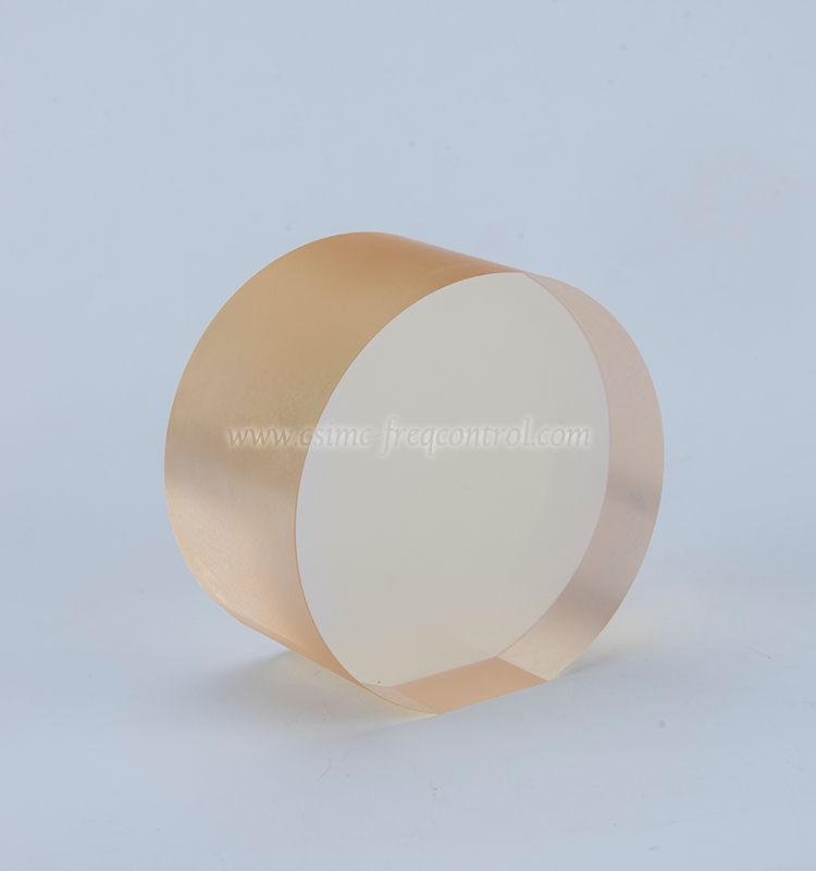
The image above shows the type of wafer presentation buyers may review during supplier evaluation. However, a product photograph cannot prove flatness, orientation, roughness, or defect limits. These properties require measurement records. Ask for a sample inspection report before approving a production lot.
State whether the wafer will be used for a SAW filter, optical modulator, infrared detector, pyroelectric sensor, or another device. The same LiTaO3 material may require a different cut and surface finish for each application.
Common development sizes may include 2-inch, 3-inch, 4-inch, and larger formats, but availability varies by supplier and process. Select the diameter based on the fabrication line, not only on the lowest unit price. A wafer that does not fit the lithography, bonding, or cleaning tool can create additional processing cost.
Do not write only “lithium tantalate wafer” on a purchase order. Include the crystal cut, orientation, rotation angle, and tolerance. For SAW work, the cut directly affects acoustic behavior. For optical work, it affects the electro-optic coefficient and polarization direction.
Define thickness tolerance, TTV, flatness, bow, warp, roughness, particle limits, scratches, pits, and edge exclusion. If the wafer will receive a thin film, state whether the polished surface must meet a specific RMS roughness value.
Request dielectric properties at the intended test frequency and temperature. Also confirm the supplier’s Curie-temperature data, operating-temperature recommendation, and any composition control. Published values are useful for early design, but lot-specific data are better for production decisions.
Use a small sample lot to test cleaning, bonding, lithography, electrode deposition, etching, and device performance. Record yield, center-frequency spread, insertion loss, optical loss, or sensor response. This gives a stronger supplier comparison than a catalog description.
Ask how the supplier controls crystal growth, slicing, lapping, polishing, cleaning, inspection, and packaging. Useful documents include a certificate of analysis, inspection map, material safety information, process flow, and change-notification policy.
A visually identical wafer can perform differently if the cut or axis direction is wrong. Confirm the orientation using an X-ray diffraction, optical, or other documented method. The certificate should state the tolerance, not only the nominal cut.
Frequency variation may result from thickness variation, electrode non-uniformity, crystal properties, temperature, or process stress. Compare wafer TTV and flatness data with the measured device map. If the variation follows wafer thickness, tighter geometry control may be required.
Particles, organic residue, roughness, and poor flatness can reduce bonding strength or cause coating defects. Confirm the cleaning process and surface condition. If the wafer is shipped in a protective film or cassette, verify that the packaging does not add residue.
Cracks can be related to edge chips, handling stress, thermal shock, or an unsuitable thickness. Inspect the edge before processing and control the temperature ramp. A supplier should provide an edge-quality standard and reject criteria.
Possible causes include surface scattering, absorption, crystal defects, contamination, or an unsuitable orientation. Request optical transmission or loss data measured at the intended wavelength. A general material datasheet cannot replace application-specific testing.
Repeatability is essential for high-volume manufacturing. Compare at least two or three lots and review the spread in thickness, flatness, roughness, and device results. A supplier that provides lot traceability can help identify the cause of a later yield change.
These advantages are useful only when the wafer matches the design. A material with strong piezoelectric performance may still fail a project if it has the wrong cut, poor flatness, excessive particles, or insufficient lot control.
| Material | Common strengths | Selection concerns |
|---|---|---|
| Lithium tantalate | Piezoelectric, pyroelectric, electro-optic, and optical functions in one crystal. | Cut, temperature behavior, surface quality, and composition must be controlled. |
| Lithium niobate | Strong electro-optic and nonlinear optical performance; widely used in photonics. | Different acoustic, optical, and temperature characteristics may change the device design. |
| Quartz | Good frequency stability and low temperature coefficient for selected cuts. | Its piezoelectric and electro-optic behavior may not meet every application need. |
| Aluminum nitride | Thin-film integration, high acoustic velocity, and semiconductor process compatibility. | Its performance depends strongly on film stress, texture, thickness, and deposition control. |
The best material is determined by the target frequency, bandwidth, temperature range, optical wavelength, power level, process flow, and cost per usable die. Comparison should be based on measured device data rather than material reputation alone.
A clear request for quotation reduces back-and-forth communication. Include the following information:
For a development project, also include the electrode metal, bonding method, deposition process, operating temperature, target frequency, optical wavelength, or sensor bandwidth. These details help the supplier recommend a practical wafer specification.
The main uses include SAW filters, RF components, pyroelectric infrared sensors, electro-optic modulators, optical switches, and nonlinear optical devices. The correct use depends on the wafer cut, orientation, thickness, and surface quality.
No. Both are ferroelectric crystals with piezoelectric and electro-optic properties, but their acoustic, optical, dielectric, and thermal parameters differ. A device designed for lithium niobate should not be transferred to lithium tantalate without new simulation and testing.
There is no single best cut for every SAW filter. The required cut depends on center frequency, coupling, bandwidth, temperature coefficient, propagation direction, and electrode structure. The final choice should come from device simulation and sample testing.
Select a diameter that matches the equipment in your fabrication line and provides the required number of usable dies. A larger wafer can improve output per run, but only when the process tool, handling system, and inspection equipment support it.
The required value depends on the application and process. Optical waveguides and thin-film bonding generally need tighter surface control than some basic sensor structures. Specify the roughness measurement method, scan length, and polished side in the purchase document.
Store wafers in clean, sealed packaging with controlled handling. Avoid direct contact with the polished surface, high-particle environments, and rapid temperature changes. Follow the supplier’s recommended temperature, humidity, and unpacking procedure.
Many suppliers can customize diameter, thickness, crystal cut, orientation, polishing, cleaning, edge shape, and packaging. Custom specifications may require a sample approval process and a minimum order quantity.
Useful documents include a certificate of analysis, wafer inspection report, orientation record, thickness and TTV data, surface-defect results, packaging details, and lot traceability. For regulated or high-reliability projects, also request the supplier’s quality-system and change-notification information.
Begin by writing the device requirements in measurable terms: frequency, bandwidth, temperature range, optical wavelength, wafer size, thickness, flatness, roughness, and allowable defects. Then request a technical quotation and sample lot from a qualified supplier. Test the wafers in the real process, record wafer-to-wafer variation, and compare usable die yield before approving volume production.
For further technical discussion, sample evaluation, and custom wafer requirements, contact CQT and ask for a lithium tantalate wafer specification sheet, inspection data, and application-matched samples. Buyers comparing lithium tantalate wafer suppliers for high-frequency devices should review both the material certificate and the measured device results before making the final decision.


Copyright © Hangzhou Freqcontrol
Electronic Technology Ltd.
All Rights Reserved | Sitemap |
Powered by 







 中文


