Quantum photonics is rapidly developing as a promising approach for quantum computing, quantum communication, and precision sensing. Unlike classical optical systems, quantum photonic platforms rely on controlling individual photons, entangled states, and quantum interference with extremely high accuracy.
To achieve practical quantum photonic systems, researchers need materials that can provide:
Efficient generation of quantum light sources
Low-loss optical transmission
High-speed photon manipulation
Precise phase and frequency control
Scalable wafer-level manufacturing
Among various photonic materials, lithium niobate (LiNbO₃) wafers have attracted significant attention because of their outstanding electro-optic properties, strong nonlinear optical response, broad optical transparency, and compatibility with integrated photonic circuits. Thin-film lithium niobate (TFLN) and lithium niobate on insulator (LNOI) platforms have further expanded its potential for next-generation quantum photonic devices.
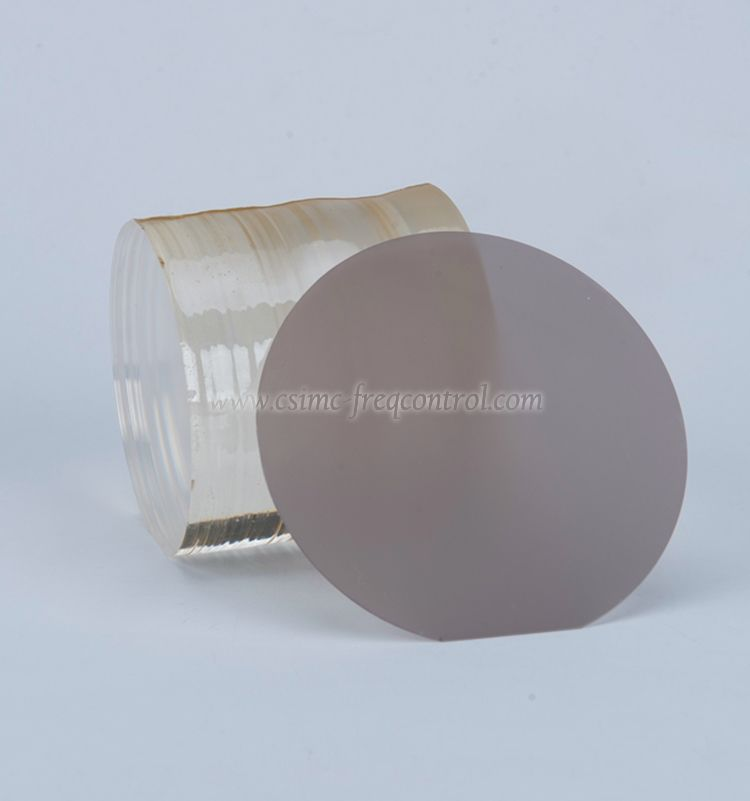
Lithium niobate wafers are crystalline substrates made from lithium niobate material, a ferroelectric compound known for its excellent optical and electrical properties.
For decades, lithium niobate has been widely used in:
Optical modulators
Frequency converters
Telecommunication components
Acousto-optic devices
Nonlinear optical systems
With the development of thin-film fabrication technologies, lithium niobate wafers can now support highly integrated photonic circuits with nanoscale waveguides and compact device structures.
Compared with traditional bulk lithium niobate crystals, thin-film lithium niobate wafers provide:
Stronger optical confinement
Smaller device footprints
Higher nonlinear interaction efficiency
Better scalability for integrated circuits
These advantages make lithium niobate wafers an important platform for quantum photonics applications.
One of the biggest challenges in quantum photonics is producing reliable quantum light sources.
Quantum systems often require:
Single photons
Photon pairs
Entangled photons
Squeezed light states
Lithium niobate wafers provide strong second-order nonlinear optical effects (χ²), enabling efficient processes such as:
Spontaneous parametric down-conversion (SPDC)
Second harmonic generation
Sum-frequency generation
Difference-frequency generation
Through SPDC, a high-energy photon can be converted into two correlated photons, creating the foundation for many quantum communication and computing applications.
Lithium niobate-based quantum photonic chips have demonstrated high-brightness photon-pair generation and integrated quantum light sources.
Quantum photonic systems require extremely precise control of photon states.
Lithium niobate is especially valuable because of its strong Pockels effect, allowing electrical signals to directly control optical properties without generating significant thermal noise.
Lithium niobate wafers enable:
High-speed optical phase modulation
Amplitude modulation
Quantum state manipulation
Programmable photonic circuits
Compared with thermo-optic approaches commonly used in other materials, electro-optic modulation in lithium niobate provides faster response times and lower energy consumption.
This makes lithium niobate an ideal material for controlling quantum bits encoded in:
Photon phase
Polarization
Time-bin states
Frequency states
Traditional quantum optical experiments often require large optical tables filled with:
Lasers
Mirrors
Beam splitters
Optical fibers
Detectors
Although these systems can demonstrate quantum effects, they are difficult to scale.
Lithium niobate wafers enable researchers to integrate multiple optical components onto a single chip, including:
Optical waveguides
Couplers
Resonators
Modulators
Frequency converters
This integration helps create compact and stable quantum photonic systems suitable for commercial applications.
Thin-film lithium niobate technology allows submicron waveguides and dense photonic integration, significantly improving scalability compared with conventional lithium niobate devices.
Quantum communication relies on transmitting quantum states of light while maintaining coherence and minimizing losses.
Lithium niobate wafers contribute to quantum communication through:
Lithium niobate photonic devices can generate and manipulate quantum states required for secure encryption systems.
Different quantum systems may operate at different wavelengths. Lithium niobate enables wavelength conversion while preserving quantum properties.
This capability helps connect:
Quantum processors
Optical fiber networks
Quantum memories
Photon detectors
Research has demonstrated lithium niobate-based quantum frequency conversion platforms with efficient conversion and low-noise operation.
Photonic quantum computing requires large numbers of precisely controlled optical components.
Lithium niobate wafers support quantum computing architectures through:
Lithium niobate photonic circuits can create programmable interferometers for manipulating photon states.
Electro-optic modulators and nonlinear components enable:
Qubit encoding
Quantum gate operations
Photon routing
Lithium niobate can potentially integrate with:
Silicon photonics
Superconducting detectors
Quantum emitters
This creates opportunities for scalable quantum processors combining different technologies.
Beyond computing and communication, lithium niobate wafers also support quantum sensing applications.
Potential applications include:
Precision measurement
Optical frequency standards
Quantum-enhanced imaging
Magnetic field sensing
The wide optical transparency range and excellent electro-optic properties allow lithium niobate devices to operate across different wavelength regions.
| Material | Advantages | Limitations |
|---|---|---|
| Silicon | Mature semiconductor manufacturing | Weak nonlinear optical response |
| Silicon Nitride | Low optical loss | Limited electro-optic functionality |
| Glass | Low cost and good transparency | Limited active modulation |
| Lithium Niobate | Strong nonlinear effects, fast modulation, wide transparency | More complex fabrication |
Lithium niobate stands out because it combines:
Nonlinear optics
Electro-optic control
Low optical loss
Wafer-scale integration capability
This combination is difficult to achieve with other photonic materials.
For researchers and manufacturers developing quantum photonic devices, important wafer specifications include:
Common orientations include:
X-cut lithium niobate wafers
Y-cut lithium niobate wafers
Z-cut lithium niobate wafers
The selection depends on:
Device design
Electric field direction
Optical polarization requirements
Thin-film lithium niobate devices typically require precise control of:
Lithium niobate layer thickness
Buried oxide thickness
Substrate properties
These parameters directly influence waveguide performance.
Important specifications include:
Surface roughness
Flatness
Defect density
Thickness uniformity
High-quality wafer surfaces are essential for low-loss optical circuits.
Quantum photonic applications often require wafers compatible with:
Electron beam lithography
Photolithography
Etching processes
Wafer bonding
The future development of lithium niobate quantum photonics is focused on:
Moving from laboratory prototypes toward commercial production requires:
Larger wafer sizes
Improved uniformity
Higher fabrication yield
Future quantum chips may combine lithium niobate with:
Silicon photonics
Quantum dots
Single-photon detectors
Cryogenic components
The ultimate goal is to develop complete quantum photonic platforms integrating:
Quantum light generation
Photon manipulation
Detection
Control electronics
on a single chip.
Lithium niobate wafers have become one of the most promising material platforms for quantum photonics because they combine strong nonlinear optical performance, fast electro-optic control, and compatibility with integrated photonic manufacturing.
From quantum communication and quantum computing to advanced sensing technologies, lithium niobate-based devices provide the essential building blocks needed for scalable quantum systems.
As thin-film lithium niobate technology continues to mature, lithium niobate wafers are expected to play an increasingly important role in transforming quantum photonics from laboratory research into practical commercial technologies.



Copyright © Hangzhou Freqcontrol
Electronic Technology Ltd.
All Rights Reserved | Sitemap |
Powered by 







 中文


