Lithium Niobate Wafers are helping engineers reduce the size of photonic, radio frequency, optical communication, and quantum devices without sacrificing high-speed performance. This guide explains why thin-film lithium niobate is attracting attention, how to evaluate it, how to design and process devices, and how purchasing teams can avoid costly material and integration mistakes.
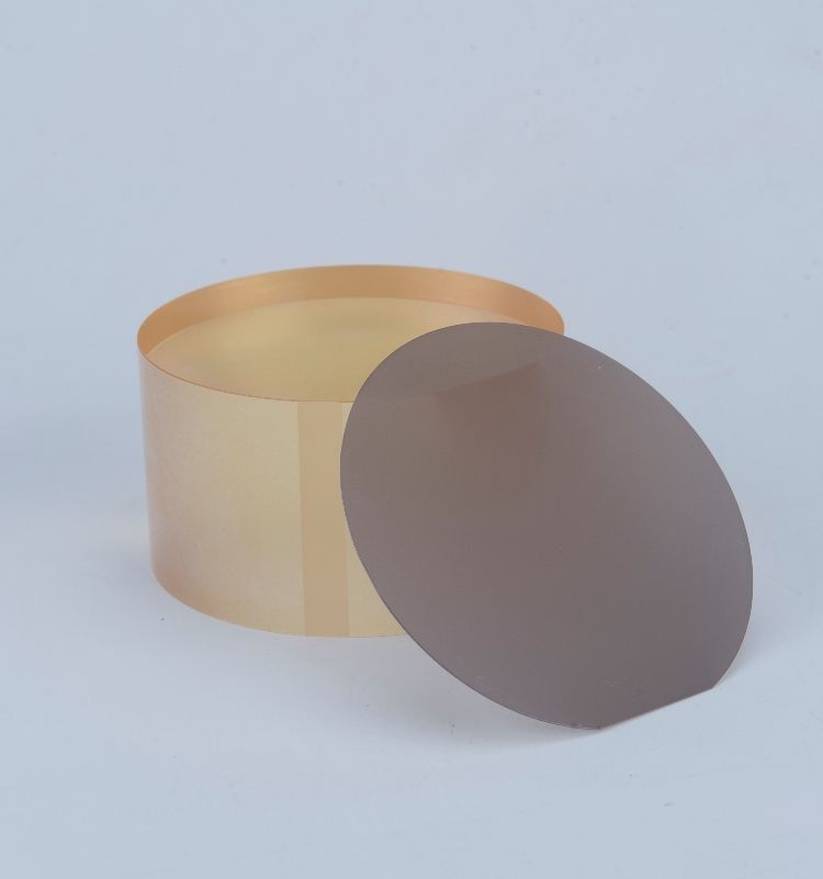
Thin-film lithium niobate solves the main limits of conventional device scaling
Why engineers are moving from bulk lithium niobate to thin-film platforms
Conventional bulk lithium niobate remains valuable for modulators, acoustic devices, and frequency control components. However, its relatively large optical mode size and limited vertical confinement can make further miniaturization difficult. Thin-film lithium niobate places a thin active layer on an insulating substrate, creating stronger field confinement and allowing smaller device structures.
- Higher optical confinement supports compact waveguides and resonators.
- Strong electro-optic response enables high-speed modulation with short interaction lengths.
- Low optical loss supports narrow-linewidth and high-efficiency devices.
- Large bandwidth makes the material suitable for advanced communication systems.
- Low microwave and optical interaction length can reduce overall electrode size.
- Compatibility with silicon dioxide, silicon, and selected semiconductor processing methods supports hybrid integration.
What purchasing groups want to confirm before approving a wafer
Purchasing groups are usually not looking for a general description of lithium niobate. They need evidence that the material can meet process, performance, supply, and cost requirements at production scale.
- Wafer diameter and usable area for the intended process.
- Lithium niobate film thickness and thickness uniformity.
- Crystal orientation, such as X-cut, Y-cut, or Z-cut.
- Surface roughness, flatness, bow, and total thickness variation.
- Optical loss and material quality for the target wavelength.
- Bonding quality between the lithium niobate film and the substrate.
- Defect density, particles, cracks, edge exclusion, and inspection standards.
- Availability of small prototype lots and repeat production lots.
- Documentation, traceability, inspection data, and technical support.
- Total cost after fabrication yield, not only the quoted wafer price.
Thin-film lithium niobate improves miniaturization through stronger device control
How the thin-film structure reduces device dimensions
A thin lithium niobate layer confines light near the device surface. Engineers can then define waveguides with lithography and etching instead of relying only on large bulk structures. This makes it possible to place multiple optical functions on one chip.
- Light enters a nanoscale or microscale lithium niobate waveguide.
- The thin film confines the optical mode in the vertical direction.
- Patterned waveguides control the horizontal mode profile.
- Electrodes are placed close to the optical mode to improve modulation efficiency.
- Multiple resonators, splitters, filters, and modulators are integrated on the same die.
- The finished photonic circuit occupies less space than a collection of discrete bulk components.
Which device categories benefit most from miniaturization
- High-speed optical modulators for data centers and telecommunications.
- Integrated frequency comb sources and wavelength converters.
- Microring resonators and narrowband optical filters.
- Photonic integrated circuits for sensing and spectroscopy.
- Quantum photonic circuits and single-photon control components.
- Acousto-optic and electro-acousto-optic devices.
- Microwave photonic signal processors.
- Compact gyroscopes, inertial sensors, and timing systems.
- Piezoelectric radio frequency and frequency control devices.
Choose wafer specifications by matching them to the device design
Start with the optical and electrical requirements
The correct wafer is determined by the device architecture, not by film thickness alone. Before requesting a quotation, define the operating wavelength, waveguide geometry, electrode design, target bandwidth, optical power, and packaging method.
- Define the operating wavelength, such as visible, near infrared, or telecom infrared.
- Set the target propagation loss and insertion loss.
- Determine the required modulation bandwidth and drive voltage.
- Choose the crystal cut based on the desired electro-optic tensor and electrode orientation.
- Estimate the required lithium niobate film thickness from the waveguide mode profile.
- Define the buried oxide thickness needed for optical isolation.
- Confirm the substrate type and its compatibility with thermal processing.
- Specify wafer size, edge exclusion, surface finish, and inspection requirements.
Review the specifications that directly affect yield
- Crystal orientation: The cut changes the effective electro-optic coefficient and affects electrode placement.
- Film thickness: Thickness variation changes optical confinement, effective index, and resonance wavelength.
- Buried oxide thickness: An inadequate oxide layer can increase substrate leakage and optical loss.
- Surface roughness: Roughness can scatter light and reduce the quality factor of resonators.
- Wafer bow: Excessive bow can create lithography focus errors and bonding problems.
- Film stress: Stress can lead to cracking, delamination, or dimensional instability during heating.
- Bonding interface: Voids and contamination can reduce yield and create local optical defects.
- Particle level: Particles can cause resist defects, etch failures, and local electrical shorts.
Use a supplier comparison table before placing an order
| Evaluation item |
Questions to ask |
Why it matters |
| Wafer structure |
What are the film, oxide, and substrate materials? |
The stack determines optical confinement and process compatibility. |
| Crystal cut |
Is the wafer X-cut, Y-cut, or Z-cut? |
The cut affects modulation efficiency and device orientation. |
| Uniformity |
What are the thickness and flatness tolerances? |
Uniformity affects yield across the entire wafer. |
| Surface quality |
What are the roughness, particle, and scratch limits? |
Surface defects can increase optical loss and reduce process yield. |
| Reliability |
What thermal cycling and storage data are available? |
Reliability data helps predict packaging and field performance. |
| Supply |
Can the supplier support prototype and production volumes? |
A material that cannot scale may create a later redesign risk. |
| Documentation |
Are certificates, maps, and inspection reports included? |
Traceability supports quality control and customer qualification. |
Follow a controlled workflow from wafer selection to miniaturized device
First step: define the device performance target
Write a measurable specification before choosing a process flow. Include optical loss, bandwidth, drive voltage, resonant wavelength, temperature range, chip size, power consumption, and expected production volume.
- Set the target chip footprint.
- Set the maximum acceptable optical loss.
- Set the target electro-optic bandwidth.
- Set the maximum drive voltage.
- Set the required operating temperature range.
- Set the acceptable prototype and production yield.
Second step: select the wafer stack and crystal orientation
Match the crystal orientation and film thickness to the optical and electrical layout. Confirm that the supplier can provide a wafer map and measured data for thickness, roughness, bow, and bonding quality.
- Select the wafer diameter required by the fabrication facility.
- Choose the lithium niobate film thickness based on the optical mode design.
- Choose the buried oxide thickness to limit substrate leakage.
- Select the crystal cut according to the dominant electro-optic interaction.
- Confirm substrate compatibility with cleaning, lithography, etching, and annealing.
- Approve the material only after reviewing representative inspection data.
Third step: create the optical and electrode layout
Design the waveguides, bends, couplers, resonators, electrodes, alignment marks, and test structures together. A waveguide that performs well optically may still be difficult to modulate if the electrode spacing is too large or the microwave design is not impedance matched.
- Define the waveguide width and height using an electromagnetic mode solver.
- Check single-mode operation at the intended wavelength.
- Set the minimum bend radius to limit radiation loss.
- Design grating couplers or edge couplers for optical input and output.
- Place electrodes close enough to improve overlap with the optical mode.
- Calculate microwave impedance and electrode loss.
- Add alignment marks and process control structures.
- Add test devices for propagation loss, extinction ratio, bandwidth, and resonance shift.
Fourth step: prepare the wafer surface
Surface preparation is essential because particles and organic contamination can affect resist adhesion, etch uniformity, bonding integrity, and optical loss.
- Inspect the wafer under optical magnification.
- Record scratches, particles, edge defects, and visible bonding voids.
- Clean the wafer using a process approved for the wafer stack.
- Dry the wafer without leaving water marks or residue.
- Use a dehydration bake if required by the resist process.
- Measure the surface condition before lithography.
Fifth step: pattern the waveguides and active structures
Electron beam lithography is often used for high-resolution prototypes, while deep ultraviolet or other advanced lithography methods may be selected for higher volume manufacturing. The process must control sidewall roughness because etched sidewalls directly affect optical scattering.
- Apply the selected resist at a controlled spin speed and bake condition.
- Measure resist thickness across the wafer.
- Align the pattern to the crystal orientation and electrode direction.
- Expose waveguides, resonators, couplers, and alignment structures.
- Develop the resist using a controlled time and temperature.
- Inspect critical dimensions before etching.
- Use a qualified dry etch process to transfer the pattern into lithium niobate.
- Measure etch depth, sidewall angle, roughness, and feature width.
Sixth step: fabricate electrodes and passive layers
Electrode fabrication must balance low electrical resistance, low optical absorption, microwave performance, and adhesion. Metal thickness, gap spacing, and dielectric coverage can strongly affect device bandwidth and drive voltage.
- Clean the etched surface without damaging the waveguide.
- Deposit an adhesion layer if it is compatible with the optical design.
- Deposit the primary electrode metal to the required thickness.
- Pattern the electrodes using lift-off or an etch-back process.
- Inspect metal continuity, edge definition, and contact pad dimensions.
- Add passivation or cladding if required by reliability and packaging.
- Check that the optical mode does not overlap excessively with absorbing metal.
Seventh step: dice, package, and test the device
Packaging can determine whether the benefits of thin-film lithium niobate are preserved in the final product. Optical coupling, thermal expansion, electrical parasitics, and mechanical stress must be controlled.
- Dice the wafer using a process that limits edge chipping.
- Clean the die and inspect the input and output facets.
- Mount the die on a carrier with controlled mechanical stress.
- Align fibers or optical elements to the couplers.
- Connect high-frequency electrodes with short, low-inductance interconnects.
- Measure optical insertion loss and propagation loss.
- Measure modulation bandwidth, extinction ratio, and drive voltage.
- Run thermal, humidity, vibration, and aging tests when required.
- Compare measured data with the original device specification.
Use the right tools to reduce design and process uncertainty
Required design and simulation tools
- Optical mode solver for waveguide dimensions and confinement.
- Finite difference or finite element electromagnetic software.
- Microwave simulation software for electrode impedance and bandwidth.
- Layout software with design rule checking.
- Thermal simulation software for package and device temperature behavior.
- Statistical data analysis software for wafer uniformity and yield.
Required wafer processing tools
- Optical microscope for surface and pattern inspection.
- Spin coater for resist application.
- Hot plates or ovens for controlled baking.
- Electron beam or photolithography system.
- Wet bench for approved cleaning and development processes.
- Dry etch system suitable for lithium niobate.
- Metal deposition system for electrodes.
- Profilometer or atomic force microscope for film and etch measurements.
- Scanning electron microscope for critical dimension inspection.
- Wafer bow and thickness measurement system.
Required optical, electrical, and reliability test tools
- Tunable laser for wavelength-dependent measurements.
- Optical power meter and fiber alignment stage.
- Optical spectrum analyzer.
- Vector network analyzer for high-frequency characterization.
- Pulse pattern generator and high-speed oscilloscope.
- Temperature controller or thermal chamber.
- Probe station for wafer-level electrical and optical testing.
- Fiber inspection microscope and connector cleaning tools.
- Environmental chamber for humidity and temperature cycling.
Compare thin-film lithium niobate with other integration platforms
Thin-film lithium niobate versus bulk lithium niobate
- Thin-film structures generally provide stronger vertical optical confinement.
- Thin-film structures support smaller waveguide bends and more compact circuits.
- Bulk lithium niobate can offer simpler processing for some large-area devices.
- Bulk devices may be easier to package when large optical apertures are required.
- Thin-film devices require tighter control of bonding, etching, and surface quality.
Thin-film lithium niobate versus silicon photonics
- Lithium niobate provides a strong electro-optic effect for high-speed modulation.
- Silicon offers mature manufacturing infrastructure and dense passive integration.
- Thin-film lithium niobate can be integrated with silicon to combine active and passive functions.
- Silicon may be preferred for highly complex digital photonic circuits.
- Lithium niobate may be preferred when low drive voltage, high bandwidth, or low optical loss is the priority.
Thin-film lithium niobate versus indium phosphide
- Indium phosphide supports integrated light generation and amplification.
- Lithium niobate is especially strong for modulation, frequency conversion, and low-loss optical control.
- Hybrid integration may combine an indium phosphide light source with a lithium niobate modulator.
- The final choice depends on whether the design prioritizes laser integration, modulation, loss, or manufacturing scale.
A purchasing checklist helps prevent expensive material and supply problems
Confirm technical acceptance criteria in writing
Do not rely on a general material name or a single nominal thickness. Create an acceptance document that defines the exact wafer structure and the inspection method for every critical parameter.
- Wafer diameter and thickness.
- Lithium niobate film thickness range.
- Film thickness uniformity across the usable area.
- Crystal cut and orientation tolerance.
- Substrate material and resistivity where applicable.
- Buried oxide thickness and uniformity.
- Surface roughness and flatness.
- Bonding void limit and defect map.
- Particle, scratch, crack, and edge exclusion limits.
- Packaging, labeling, and storage conditions.
Evaluate supplier capability beyond the initial quotation
The lowest unit price may not produce the lowest project cost. Purchasing groups should evaluate development support, lot consistency, replacement policy, lead time, and the supplier's ability to provide technical records.
- Request a representative sample or engineering lot.
- Review the certificate of analysis and wafer inspection map.
- Process the sample using the intended fabrication flow.
- Measure yield, optical loss, dimensional stability, and device performance.
- Compare results with the supplier's stated specifications.
- Ask how nonconforming wafers are handled.
- Confirm prototype lead time and production lead time separately.
- Review capacity, second-source options, and change notification procedures.
- Approve the supplier only after technical and commercial review.
Work with CQT when consistency and documentation are purchasing priorities
CQT can be considered as a technical partner for teams that need a clear specification process for Lithium Niobate Wafers. A practical supplier evaluation should include wafer structure, crystal orientation, surface quality, thickness uniformity, inspection records, packaging, and long-term supply planning.
When contacting CQT, provide the device application, operating wavelength, required wafer size, film thickness, crystal cut, substrate structure, target quantity, and intended fabrication process. This information allows the quotation and technical review to focus on the parameters that affect device yield rather than only the nominal wafer price.
Avoid common mistakes that reduce miniaturization benefits
Do not choose film thickness without running a mode analysis
A film that is too thin may provide weak confinement and poor electrode overlap. A film that is too thick may support unwanted modes or require larger waveguide dimensions. Simulate the optical mode before finalizing the wafer specification.
Do not ignore the relationship between crystal cut and electrode direction
The electro-optic response depends on crystal orientation and field direction. Incorrect alignment can reduce modulation efficiency and increase drive voltage even when the wafer itself meets its nominal specification.
Do not treat surface roughness as a cosmetic parameter
Roughness can increase scattering loss, reduce resonator quality factor, and create inconsistent results across the wafer. Require a defined roughness measurement method and inspect representative locations.
Do not use an etch process without sidewall characterization
Etch depth, sidewall angle, residue, and roughness can change the effective index and optical loss. Measure etched test structures before moving to a full production layout.
Do not place metal too close to the optical mode without checking absorption
Close electrodes improve electro-optic interaction, but excessive optical overlap with metal can increase absorption and heating. Optimize electrode spacing with both optical and microwave simulations.
Do not evaluate only one die from one wafer location
Thin-film uniformity and process variation can affect performance across the wafer. Test center, middle-radius, and edge locations to understand the real process window.
Do not postpone packaging design
A compact photonic circuit can lose its performance advantage through long electrical connections, poor fiber alignment, thermal stress, or an oversized package. Include packaging constraints during the first layout iteration.
Use a qualification plan to move from prototype to production
First phase: verify material and process compatibility
- Inspect incoming wafers and compare them with the acceptance criteria.
- Run cleaning, lithography, etching, and metal deposition trials.
- Measure film thickness, surface roughness, etch profile, and bonding defects.
- Record every process condition that affects yield.
Second phase: verify device performance
- Measure optical loss and coupling efficiency.
- Measure resonant wavelength and thermal shift.
- Measure modulation bandwidth and drive voltage.
- Measure electrical resistance, impedance, and microwave loss.
- Compare results across multiple wafer locations.
Third phase: verify reliability and supply continuity
- Perform thermal cycling and humidity testing.
- Evaluate optical and electrical performance after aging.
- Confirm packaging and storage requirements.
- Review lot-to-lot uniformity.
- Confirm production capacity and expected lead time.
- Establish change control, traceability, and nonconformance procedures.
With a controlled design, fabrication, and purchasing process, Lithium Niobate Wafers can support smaller, faster, and more integrated devices across optical communication, sensing, frequency control, and quantum applications. Working with a qualified supplier such as CQT helps engineering and purchasing teams connect material specifications with real device performance and dependable production planning.









 中文


