A Quartz Glass Substrate is a flat, high-purity fused-silica component used in semiconductor equipment, optical systems, RF devices, sensors, and laboratory instruments. Unlike ordinary glass, it is designed to control thermal expansion, chemical stability, surface flatness, and particle levels. Engineers looking for a high purity quartz glass substrate for semiconductor processing must consider material grade, thickness, surface finish, cleaning, and inspection—not only the purchase price. This guide explains how quartz substrates work, where they are used, and how to select a reliable supplier such as CQT.
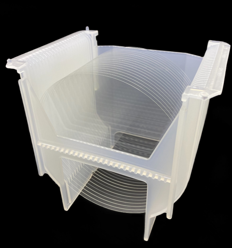
A Quartz Glass Substrate is a plate, wafer, disc, window, or custom-shaped part made from fused silica. Fused silica is mainly silicon dioxide, or SiO2, produced by melting or depositing high-purity silica and then forming it into a controlled shape.
In industry, the terms “quartz glass” and “fused silica” are often used in similar ways. However, the manufacturing route can affect purity, hydroxyl content, optical transmission, thermal behavior, and performance at high temperature. A supplier should therefore provide a material specification instead of relying only on the word “quartz.”
Purity: The concentration of metallic and other unwanted impurities. Low levels of iron, sodium, potassium, and other contaminants are important in semiconductor and optical applications.
Thermal expansion: Fused silica has a very low coefficient of thermal expansion. Corning reports a typical value of about 0.55 × 10⁻⁶/°C for fused silica near room temperature, although the exact value depends on grade and temperature range.
Softening point: Quartz glass can tolerate high processing temperatures, but it is not immune to deformation. The working temperature, load, heating rate, and cooling rate must all be controlled.
Surface roughness: This describes small surface height changes, often measured as Ra or RMS. A lower value may be needed for thin-film coating, photolithography, and optical use.
Flatness and parallelism: Flatness controls the shape of one surface, while parallelism compares the relationship between two surfaces. Both affect wafer handling, coating thickness, and alignment.
Hydroxyl content: OH groups in fused silica can influence infrared absorption and high-temperature behavior. The correct OH level depends on the application.
Thermal shock resistance: Low expansion reduces stress during temperature changes, but poor handling, sharp corners, scratches, and uneven heating can still cause cracking.
Many industrial processes combine high heat, aggressive chemicals, ultraviolet light, vacuum, and strict particle control. Common materials may expand, corrode, release contaminants, or lose optical performance under these conditions.
Quartz glass addresses several of these risks:
Its low thermal expansion helps reduce dimensional change during heating and cooling.
Its chemical resistance supports use with many acids, solvents, and process gases. The exact compatibility must still be confirmed for each chemical and temperature.
Its optical transmission extends from the ultraviolet region into the infrared, depending on material grade, thickness, and impurity level.
Its electrical insulation makes it suitable for dielectric supports, sensor parts, and high-frequency assemblies.
Its low metal contamination potential supports cleanroom and semiconductor processes when it is properly manufactured, cleaned, packed, and handled.
These properties do not automatically guarantee process success. A substrate with the right chemical composition can still fail if its edge is chipped, its surface is contaminated, or its flatness does not match the equipment tolerance.
Quartz glass is hard, brittle, and sensitive to surface damage. It does not behave like aluminum, stainless steel, or standard optical glass during cutting and polishing. A small scratch can become a crack when the part is heated, clamped, or exposed to vibration.
Cutting creates mechanical and thermal stress. Incorrect blade selection, excessive feed speed, poor coolant control, or weak workholding can produce edge chips and microcracks. These defects may not be visible during a quick visual check, but they can grow during later heating cycles.
Common controls include diamond tools, stable fixturing, suitable coolant flow, low-vibration equipment, and a defined edge profile. The drawing should state corner radius, chamfer size, edge exclusion, and allowable chips.
Polishing must remove subsurface damage without creating waviness or edge roll-off. A substrate may meet a roughness target but still fail because its overall flatness is outside the equipment requirement.
For this reason, a technical drawing should separate:
Surface roughness, such as Ra or RMS;
Total thickness variation, or TTV;
Local and global flatness;
Parallelism;
Edge exclusion and usable area.
Cleaning is not a cosmetic step. Particles, polishing residue, fingerprints, and metallic contamination can affect thin films, optical transmission, bonding, and semiconductor yield.
A controlled cleaning process may include ultrapure water rinsing, approved chemical cleaning, drying with filtered gas, visual inspection, and particle testing. The best method depends on the substrate size, coating, surface finish, and end-use process. Aggressive cleaning can also damage coatings or change surface chemistry.
Although fused silica has a low coefficient of thermal expansion, a thick substrate or a substrate with a sharp defect can still crack during rapid temperature changes. Uneven heating is especially risky. Operators should avoid placing a cold part directly on a hot metal surface and should use clean, compatible tools.
Dimensions change with temperature, even when the expansion is small. Measurement reports should state the reference temperature, measurement method, instrument resolution, and inspection area. For demanding applications, suppliers may need to provide interferometric flatness data, thickness maps, roughness measurements, and defect inspection records.
Quartz substrates are used in wafer-processing equipment, deposition systems, etching systems, thermal processing tools, and component supports. They may function as carriers, boats, windows, liners, rings, plates, or insulation parts.
In semiconductor production, the key concerns are often:
Low metallic contamination;
Stable dimensions at process temperature;
Low particle generation;
Controlled surface finish;
Compatibility with cleaning chemicals and process gases;
Repeatable geometry from batch to batch.
MEMS devices also use quartz or fused silica for optical access, sensor structures, insulating layers, and stable mechanical parts. The correct design depends on the device frequency, bonding method, electrode pattern, and thermal cycle.
A quartz glass substrate for RF filter manufacturing can provide electrical insulation, dimensional stability, and low dielectric loss compared with many conventional materials. It may be used in resonators, filter assemblies, frequency-control components, and precision insulating structures.
RF performance depends on more than the substrate material. Designers should check dielectric constant, dissipation factor, thickness tolerance, surface condition, metallization method, and operating frequency. At microwave frequencies, small dimensional errors can change impedance, resonance, or coupling.
Fused silica is widely used for optical windows, UV components, lamp envelopes, spacers, lens carriers, and photonics fixtures. Its value is linked to ultraviolet transmission, low expansion, and resistance to thermal cycling.
For optical parts, the specification may include:
Wavelength range;
Transmission or reflectance target;
Surface quality, such as scratch-dig notation;
Surface flatness;
Wedge angle;
Coating type and laser-damage threshold.
Quartz-based parts are used in timing and frequency-control systems because stable dimensions and electrical insulation are important to repeatable performance. In these systems, substrate thickness, electrode alignment, surface cleanliness, and bonding quality can influence the final frequency response.
Quartz plates and carriers can support high-temperature coating, diffusion, annealing, and deposition processes. Their low expansion helps reduce movement during thermal cycles, while their chemical resistance supports repeated cleaning.
Quartz glass is used for reaction vessels, sample holders, cuvettes, tubes, covers, and high-temperature laboratory fixtures. The required grade depends on chemical exposure, temperature, optical measurement range, and cleaning method.
| Advantage | Why It Matters | Typical Design Question |
|---|---|---|
| Low thermal expansion | Reduces dimensional change during heating and cooling. | What temperature range and flatness tolerance are required? |
| High-temperature capability | Supports thermal processing when the load and atmosphere are controlled. | Will the part be exposed to vacuum, oxygen, hydrogen, or process gases? |
| Chemical resistance | Helps the part survive cleaning and process exposure. | Which chemicals, concentrations, and exposure times are involved? |
| Optical transmission | Supports UV, visible, and selected infrared applications. | What wavelength and transmission level must be achieved? |
| Electrical insulation | Reduces unwanted current paths in sensors and RF assemblies. | Are dielectric loss and high-frequency behavior specified? |
Quartz glass is brittle and can chip during transport or assembly.
It can be scratched by unsuitable tools or abrasive particles.
It may deform under prolonged high temperature and mechanical load.
Not every grade offers the same UV or infrared transmission.
Chemical resistance is not universal; hot alkaline solutions and certain process conditions require special review.
High-precision polishing and inspection can increase cost and lead time.
Supplier selection should begin with the process conditions, not with a generic product name. Prepare a technical request that includes the following information:
Geometry: Length, width, diameter, thickness, holes, slots, grooves, and edge shape.
Material: Fused silica or quartz grade, purity level, OH content, and optical requirements.
Surface: Roughness, polish type, flatness, parallelism, coating, and allowable defects.
Environment: Temperature, pressure, vacuum level, chemicals, gases, and cycle time.
Cleanliness: Particle limits, ionic contamination limits, cleaning method, and packaging class.
Inspection: Dimensional report, thickness map, flatness report, roughness report, visual inspection, and material certificate.
Quantity: Prototype volume, monthly demand, replacement frequency, and batch consistency requirements.
Ask the supplier how it controls tool wear, edge damage, cleaning, packaging, and traceability. A supplier that can explain the full process is more useful than one that only provides a material name.
A practical incoming inspection plan may include:
Confirming part number, drawing revision, quantity, and packaging condition;
Checking length, width, diameter, thickness, hole position, and edge geometry;
Measuring flatness, TTV, and parallelism when required;
Inspecting scratches, chips, stains, cracks, bubbles, and inclusions under defined lighting;
Testing surface roughness with a calibrated instrument;
Reviewing material and purity certificates;
Checking cleanliness and particles according to the customer’s process standard;
Recording lot number and inspection results for traceability.
Inspection limits should be written before production begins. Terms such as “high purity,” “optical grade,” or “smooth surface” are not complete specifications without numerical limits and test methods.
CQT can be considered when a project requires a custom quartz component rather than an off-the-shelf plate. The discussion should cover drawing review, material selection, cutting, grinding, polishing, cleaning, inspection, packaging, and delivery.
For a new project, send CQT:
The latest 2D drawing or 3D model;
Required material grade and purity;
Operating temperature and chemical environment;
Surface roughness, flatness, and thickness tolerances;
Cleanroom or particle requirements;
Prototype quantity and expected production volume.
CQT should then confirm whether the requested tolerances match the intended process and identify any risk from thin walls, sharp internal corners, deep holes, or large unsupported areas.
The terms are often used interchangeably, but they can describe materials made by different production routes. Always verify purity, OH content, optical range, thermal properties, and the supplier’s material certificate.
No. Fused silica has strong high-temperature performance, but the safe limit depends on temperature, time, mechanical load, atmosphere, thickness, and geometry. Thermal cycling and uneven heating can cause failure even when the average temperature is acceptable.
Surface roughness can influence particle retention, coating uniformity, optical scatter, bonding, and electrical performance. The correct value depends on the application, so it should be specified with a measurement method.
Use suitable diamond tools, stable fixturing, controlled cutting conditions, rounded or chamfered edges, careful cleaning, and slow temperature transitions. Inspect edges and surfaces before thermal processing.
Include dimensions, material grade, purity, thickness, surface finish, flatness, edge details, holes, operating environment, quantity, inspection documents, packaging requirements, and delivery target.
It can be suitable for RF and microwave parts when its dielectric behavior, thickness tolerance, surface condition, and metallization process meet the circuit design. The supplier should provide or confirm the required electrical data for the operating frequency.
Store them in clean, dry packaging with edge protection. Avoid direct contact with metal tools, abrasive materials, and unclean gloves. Follow the supplier’s cleaning and handling instructions before installation.
Start with the process window: temperature, chemicals, atmosphere, wavelength, frequency, dimensions, and cleanliness. Convert each need into a measurable specification, then request a drawing review and sample plan from a qualified supplier. Read the user guide and handling instructions before testing the part, and ask CQT to review the design if the substrate includes tight flatness, thin sections, precision holes, or repeated thermal cycles. This approach makes it easier to select a custom quartz glass substrate supplier for precision applications and reduce avoidable cracking, contamination, and dimensional problems.


Copyright © Hangzhou Freqcontrol
Electronic Technology Ltd.
All Rights Reserved | Sitemap |
Powered by 







 中文


