Single Crystal Quartz Wafers are precision substrates made from one continuous quartz crystal. They support stable frequency control, surface acoustic wave devices, sensors, and semiconductor research. Unlike fused quartz, which is amorphous, a single crystal has an ordered atomic structure and defined crystal directions. This structure gives high-purity single crystal quartz wafers controlled piezoelectric and optical behavior. For engineers comparing materials, this guide explains wafer grades, production steps, processing risks, applications, and how to choose single crystal quartz wafers for semiconductor applications.
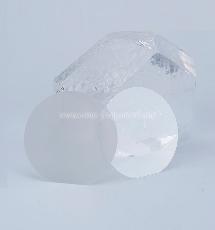
A single crystal quartz wafer is a thin, flat slice cut from a synthetic or natural quartz crystal. Quartz is crystalline silicon dioxide, written as SiO2. In a single crystal, the silicon and oxygen atoms follow one continuous lattice rather than forming many small grains.
The word “wafer” describes the shape and use of the material. It does not automatically define the crystal quality, orientation, thickness, or surface finish. A useful specification should include:
Quartz is also piezoelectric. When mechanical stress is applied, it can produce an electrical charge. The reverse is also true: an electrical field can create mechanical vibration. This effect is the operating principle behind many quartz resonators, filters, and surface acoustic wave devices.
| Property | Single crystal quartz | Fused quartz |
|---|---|---|
| Atomic structure | Ordered crystal lattice | Amorphous glass structure |
| Piezoelectric behavior | Available and orientation-dependent | Not used as a bulk piezoelectric crystal |
| Optical behavior | Can show anisotropy and birefringence | Generally isotropic |
| Thermal expansion | Depends on crystal direction | Low and more uniform in the material |
| Typical uses | Resonators, SAW devices, sensors, optical components | Laboratory ware, tubes, lamps, and high-temperature parts |
The choice depends on the device function. If the design requires a controlled resonant frequency or a crystal-axis-dependent optical response, single crystal quartz is usually the relevant material. If the main need is chemical resistance and low thermal expansion, fused quartz may be more suitable.
Quartz converts mechanical vibration into an electrical signal and electrical energy into vibration. The response changes with crystal orientation, electrode design, thickness, and temperature. This makes the cut angle a design parameter, not a cosmetic feature.
Quartz is valued for frequency stability because its elastic and thermal properties can be controlled through crystal cuts. AT-cut quartz, for example, is widely used in frequency-control devices because it can reduce the first-order frequency change over a selected temperature range. The final stability still depends on the resonator design, packaging, drive level, and temperature-compensation circuit.
Quartz has a Mohs hardness of about 7, so it resists many common scratches. It also has strong resistance to many acids and solvents. However, hydrofluoric acid and hot alkaline solutions can attack silica-based materials. Chemical compatibility must therefore be checked before wet processing.
High-quality quartz can transmit light across a broad ultraviolet, visible, and infrared range. The useful range depends on impurity content, water absorption, crystal quality, thickness, and surface coating. Optical designers should request spectral-transmission data instead of relying on a general “high-transmission” claim.
Quartz has a major phase transition near 573°C at atmospheric pressure, where alpha quartz changes to beta quartz. This transition can affect dimensions and mechanical behavior. Process temperatures should be controlled when a wafer is used in a precision resonator or repeatedly heated and cooled.
Producing a reliable quartz wafer is more than slicing a crystal into disks. Each step can change the final electrical, optical, or mechanical performance.
Synthetic quartz is often grown by the hydrothermal process. In this method, quartz dissolves in a hot, pressurized alkaline solution and recrystallizes on seed plates. The process can produce large crystals with controlled quality, but growth rate, impurity level, seed condition, and internal defects must be monitored.
Quartz is anisotropic, which means its properties vary with direction. A small orientation error can alter frequency-temperature behavior, optical polarization, or piezoelectric response. Manufacturers use methods such as X-ray diffraction, optical inspection, and orientation measurement to locate the required axis.
Diamond wire or diamond-blade equipment is used to slice the boule. Cutting creates kerf loss, subsurface damage, warpage, and thickness variation. The cutting method must balance production speed with the required thickness tolerance and edge quality.
Lapping removes saw damage and brings the wafer closer to its target thickness. Excessive pressure can create cracks or stress layers below the surface. Abrasive size, slurry concentration, carrier movement, and cleaning between steps all affect the result.
Polishing reduces roughness and removes the damaged layer left by grinding. For optical windows and high-frequency devices, a low-roughness surface can improve bonding, electrode patterning, and signal performance. A supplier should report measurement conditions because Ra and RMS values are not always directly comparable.
Particles, metal ions, organic residues, and abrasive remains can reduce yield. Cleaning may include solvent steps, ultrapure water rinsing, megasonic cleaning, or carefully controlled chemical treatment. The correct process depends on the downstream device and its contamination limits.
Final inspection can include diameter, thickness, flatness, TTV, surface roughness, edge chips, cracks, inclusions, orientation, and optical transmission. Wafers should be packed in clean containers with separators that do not scratch the polished surface.
Quartz resonators and crystal oscillators are used in clocks, communication equipment, industrial controllers, test instruments, and automotive electronics. Their frequency is determined by crystal geometry, cut orientation, electrode structure, and circuit conditions.
SAW filters use acoustic waves traveling along the surface of a piezoelectric substrate. Quartz wafers can be used when stable frequency behavior and low aging are important. The electrode pattern is normally formed by photolithography and metal deposition.
Quartz substrates are used in thin-film studies, microelectromechanical systems, sensors, and laboratory processes. Their electrical insulation, thermal behavior, and chemical resistance can be useful when researchers need a nonconductive crystalline platform.
Quartz crystal microbalance sensors measure changes in resonance frequency when mass attaches to the surface. The Sauerbrey equation is commonly used for rigid, thin, evenly distributed films:
Δf = −Cf × Δm
Here, Δf is the frequency shift, Δm is the mass change per unit area, and Cf is the mass-sensitivity constant for the crystal design. In liquid or viscoelastic films, the Sauerbrey model may not be sufficient, so additional acoustic models are needed.
Quartz plates and windows are used in optical instruments, ultraviolet systems, spectroscopy, and laser equipment. Crystal orientation, absorption, birefringence, surface flatness, and coating compatibility should be specified for each optical design.
Quartz can be selected for components that contact chemicals or require stable dimensions during temperature changes. The final choice should consider the exact chemical concentration, pressure, temperature, cleaning method, and exposure time.
These advantages only appear when the wafer matches the process. A low-roughness wafer with the wrong crystal cut may perform worse than a correctly oriented wafer with a less demanding surface finish. Material selection should therefore start with the device specification rather than a general product name.
State whether the wafer will be used for a resonator, SAW filter, sensor, optical component, thin-film experiment, or semiconductor process. Each application may require a different cut, diameter, thickness, and surface treatment.
Ask for the required cut and the permitted orientation tolerance. If the design team has not selected a cut, provide the frequency range, temperature range, electrode structure, and expected operating mode to the supplier.
Replace vague terms such as “smooth” or “premium” with measurable values. Useful requirements include:
Check whether the wafer will face vacuum deposition, plasma exposure, photolithography, thermal cycling, wet etching, bonding, or ultrasonic cleaning. Some processes can damage the edge or create contamination even when the starting wafer meets its dimensional specifications.
A technical data sheet should be supported by inspection records or a certificate of conformance. Depending on the project, request orientation data, thickness mapping, surface-roughness results, optical-transmission curves, and defect inspection records.
| Problem | Likely cause | Recommended action |
|---|---|---|
| Frequency does not match the design | Wrong cut, thickness, electrode mass, or orientation | Verify the crystal cut, dimensional tolerance, and resonator model |
| Cracks appear after processing | Subsurface grinding damage, edge chips, or thermal stress | Improve edge treatment, reduce mechanical load, and control thermal cycling |
| Film does not bond evenly | Particles, organic residue, roughness, or poor cleaning | Review cleaning, surface activation, and roughness specifications |
| Optical transmission is lower than expected | Impurities, inclusions, coating loss, or incorrect thickness data | Request wavelength-specific transmission and defect inspection results |
| Wafer breaks during handling | Thin geometry, sharp edge, internal stress, or unsuitable packaging | Use edge finishing, protective carriers, and controlled handling tools |
Quartz wafer specifications should be connected to recognized measurement methods and the final device requirement. Useful technical references include:
These sources provide general technical context. A wafer supplier must still provide product-specific data because crystal growth, orientation, polishing, and inspection methods can change the final performance.
CQT can help buyers turn a general request into a measurable wafer specification. Before requesting a quotation, prepare the target diameter, thickness, crystal cut, orientation tolerance, surface finish, flatness, roughness, edge profile, quantity, and intended process.
For a prototype, it is often useful to begin with a small batch and test the wafers through the actual deposition, bonding, or device-fabrication process. Record yield, surface defects, frequency behavior, and handling damage. This data makes later production specifications more accurate.
No. Single crystal quartz has an ordered atomic lattice and direction-dependent properties. Glass is amorphous and does not provide the same piezoelectric or anisotropic response.
Quartz is generally an electrical insulator. Conductive electrodes or deposited films are added when a device needs electrical excitation or signal collection.
There is no universal best cut. AT-cut, BT-cut, ST-cut, X-cut, and Z-cut wafers support different electrical, mechanical, and thermal behaviors. The correct choice depends on the operating mode and device design.
Yes. They can serve as substrates or process materials in research and specialized fabrication. However, the wafer must meet the process requirements for contamination, particle level, flatness, thermal exposure, and chemical compatibility.
The target depends on the application. A sensor or optical component may need a different finish from a thin-film or bonding process. Specify the roughness value, measurement method, and sampling area instead of using only the word “polished.”
Use a cleaning process approved for the wafer coating, electrodes, and downstream equipment. Quartz resists many chemicals, but hydrofluoric acid and strong alkaline conditions can etch or damage silica-based surfaces. Always validate the process on test pieces first.
Custom dimensions may be possible, depending on the crystal material, cut, thickness, tolerance, and order quantity. Send the complete drawing and inspection requirements to CQT for feasibility review.
Start by writing a one-page specification with the application, crystal orientation, wafer dimensions, surface requirements, temperature range, cleaning chemistry, and inspection data needed. Then request samples, review the certificate of conformance, and test the wafers in the real process. For additional guidance, consult the CQT product information and user documentation before placing a production order. If you need custom single crystal quartz wafers, share your drawing and process conditions with CQT so the material and inspection plan can be matched to your device.


Copyright © Hangzhou Freqcontrol
Electronic Technology Ltd.
All Rights Reserved | Sitemap |
Powered by 







 中文


