Lithium Niobate Wafers are used in optical communications, piezoelectric sensors, acoustic filters, modulators, and quantum photonics. Their value comes from a combination of strong electro-optic, piezoelectric, nonlinear optical, and acousto-optic properties. Engineers selecting a wafer must compare crystal orientation, substrate size, optical loss, surface roughness, film thickness, and electrode compatibility. This guide explains how to choose a lithium niobate wafer supplier, when to use thin-film lithium niobate wafers, and how lithium niobate wafers for piezoelectric devices perform in real production conditions.
A lithium niobate wafer is a polished slice of lithium niobate crystal, usually written as LiNbO3. It is a ferroelectric material with a non-centrosymmetric crystal structure. This structure allows the material to convert electrical energy into mechanical or optical responses.
Commercial wafers may be made from bulk lithium niobate or from a thin lithium niobate film bonded to another substrate. Common substrate choices include:
The term “wafer” describes the format. It does not describe performance by itself. Two wafers with the same diameter can produce different results because of differences in crystal cut, film thickness, surface roughness, defect density, and polishing quality.
Lithium niobate combines several useful properties in one platform:
| Property | Engineering value | Typical design impact |
|---|---|---|
| Electro-optic effect | Changes the refractive index when voltage is applied | Supports high-speed optical modulators and switches |
| Piezoelectric effect | Converts electrical signals into mechanical waves | Supports acoustic filters, resonators, and sensors |
| Nonlinear optical response | Allows light to interact and generate new frequencies | Supports frequency conversion and quantum photonics |
| Wide optical transmission range | Works across many visible and infrared designs | Supports communications, imaging, and spectroscopy |
| High Curie temperature | Provides a broad operating margin compared with many low-temperature ferroelectrics | Useful for stable device operation when thermal design is controlled |
Published material studies report strong electro-optic and nonlinear coefficients for lithium niobate. The exact value depends on wavelength, crystal cut, temperature, stoichiometry, and measurement method. For this reason, engineers should use the supplier’s certified data sheet instead of relying only on a general material table.
Choosing a piezoelectric wafer is not simply a search for the highest coupling value. Device performance depends on the complete stack: wafer, electrodes, bonding layer, acoustic cavity, packaging, and driving circuit.
Crystal orientation controls how the electric field interacts with the piezoelectric tensor. A wafer cut that works well for a surface acoustic wave device may not be the best choice for an optical modulator.
For example, an X-cut wafer can support strong in-plane electric-field interaction in some thin-film optical designs. A Z-cut wafer may be selected when the design requires a different electro-optic coefficient or vertical field arrangement. The correct choice should be confirmed with electromagnetic and finite-element simulations.
For thickness-mode piezoelectric devices, resonant frequency is strongly related to wafer thickness and acoustic velocity. A simplified relationship is:
f ≈ v / 2t
In this equation, f is the approximate thickness resonance, v is acoustic velocity, and t is wafer or film thickness. This is only a first estimate because electrodes, bonding layers, loading, and lateral dimensions also shift the resonance.
Thin films can support smaller acoustic features and higher operating frequencies. However, thinner layers usually require tighter control of film uniformity, bonding quality, and etch depth.
Rough surfaces scatter light and can reduce the quality factor of optical or acoustic devices. A supplier should provide a measured RMS roughness value, measurement area, and test method. A roughness value without these details is difficult to compare.
For integrated photonics, sidewall roughness can be as important as wafer surface roughness. A polished wafer may still produce optical loss if the lithography and etching process creates rough waveguide walls.
Defects and impurities can increase optical absorption or cause photorefractive behavior. Photorefractive damage occurs when intense light changes the refractive index through charge transport and internal electric fields. It may affect high-power or visible-light systems.
Stoichiometric material, magnesium-oxide-doped lithium niobate, and careful process control are used in some designs to reduce photorefractive sensitivity. The best option depends on wavelength, optical intensity, temperature, and device geometry.
Lithium niobate and its bonding materials do not expand at the same rate. During heating and cooling, this mismatch can create stress, wafer bow, or delamination. Engineers should review:
A wafer that performs well in a laboratory may need a different stack for volume manufacturing. Packaging conditions should therefore be included during material selection.
Lithium niobate is widely used in electro-optic modulators. An applied voltage changes the refractive index, allowing the device to control light intensity or phase. This function is important in fiber-optic transmitters, coherent communications, data-center links, and microwave photonics.
Traditional lithium niobate modulators use bulk or diffusion-based structures. Thin-film lithium niobate allows compact waveguides and tighter optical confinement. A 2018 study published in Nature demonstrated integrated lithium niobate photonic devices with low-loss waveguides and high-speed modulation potential, helping establish LNOI as a major integrated photonics platform.
The piezoelectric response of LiNbO3 allows electrodes to create acoustic waves. These waves can be used in radio-frequency filters, resonators, delay lines, and timing components.
Thin-film acoustic devices can offer high frequency operation and strong electromechanical interaction. The final filter response depends on electrode pitch, film thickness, crystal cut, acoustic reflector design, and packaging.
Lithium niobate wafers can detect pressure, vibration, acceleration, temperature-related changes, and acoustic signals. They can also produce controlled mechanical movement when driven by voltage.
These characteristics are useful in industrial monitoring, ultrasound, microfluidics, chemical sensing, and precision positioning. Sensor designers must evaluate signal drift, temperature response, electrode stability, and environmental protection.
Lithium niobate supports second-order nonlinear optical processes, including second-harmonic generation and optical parametric interactions. Periodically poled lithium niobate, often abbreviated PPLN, uses controlled domain inversion to achieve quasi-phase matching.
Quasi-phase matching improves the interaction between different optical waves by periodically correcting their phase relationship. This approach is used in laser wavelength conversion, spectroscopy, quantum light sources, and medical imaging systems.
Integrated lithium niobate platforms are being studied for quantum frequency conversion, photon-pair generation, electro-optic control, and reconfigurable photonic circuits. The material is attractive because it combines optical transparency, fast electrical control, and nonlinear interaction in one platform.
Microwave photonics uses optical components to process or transmit radio-frequency signals. Lithium niobate modulators can convert microwave information into optical signals with high linearity and wide bandwidth. Applications include radar, antenna links, satellite communications, and signal distribution.
| Comparison point | Bulk lithium niobate | Thin-film lithium niobate |
|---|---|---|
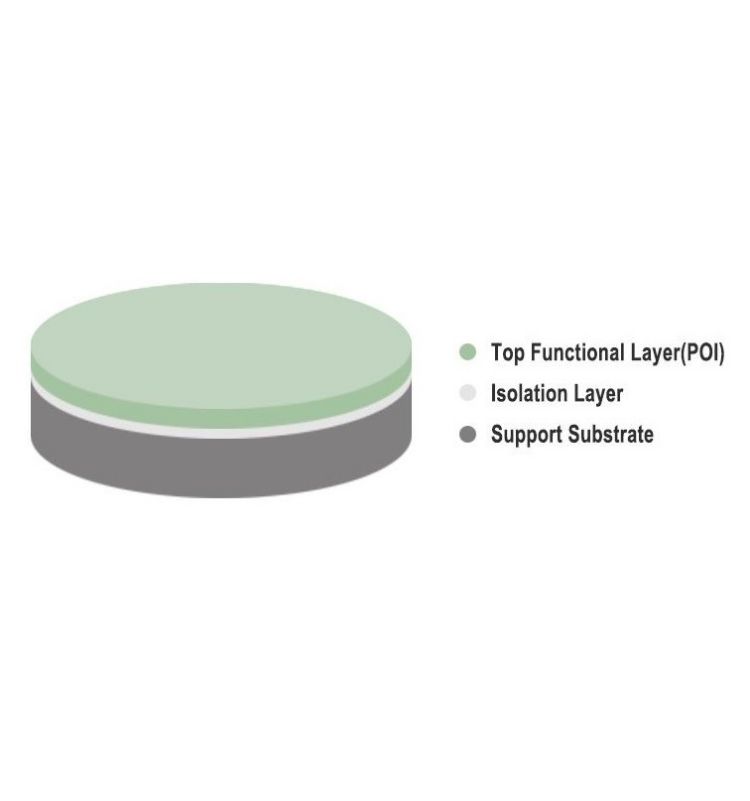
| Structure | Solid lithium niobate wafer | Thin LiNbO3 layer on an insulator and support substrate |
| Optical confinement | Usually lower without additional waveguide processing | Strong confinement is possible with nanometer- or micrometer-scale structures |
| Device size | Often larger | Compact photonic and acoustic layouts are possible |
| Processing complexity | Established processing routes | Requires bonding, thin-film control, and careful etching |
| Typical risk | Bulk defects, polishing, and domain control | Bond voids, film nonuniformity, wafer bow, and sidewall roughness |
Bulk material may be the practical choice for large-aperture optical components, conventional modulators, and some piezoelectric structures. Thin-film material is often preferred when the project needs compact integration, high optical confinement, or strong interaction between electrodes and optical modes.
A supplier comparison should begin with a technical specification sheet rather than a product image. Request the following information:
Confirm whether the wafer is compatible with your photolithography, metal deposition, dry etching, wet cleaning, bonding, and thermal treatment steps. Some processes can cause lithium out-diffusion, surface charging, or film damage if temperature and chemistry are not controlled.
Before a volume order, request engineering samples. Test them in the actual device process and measure:
A reliable lithium niobate wafer supplier should explain the test method, acceptance limits, traceability system, and replacement policy. These details reduce the risk of receiving material that meets a general specification but fails in the final device.
Possible causes include sidewall roughness, wafer contamination, absorption centers, poor fiber coupling, and mode mismatch. Measure loss with a cutback method where possible, then separate wafer loss from waveguide-processing loss.
Packaging stress, adhesive loading, electrode thickness, and temperature can change acoustic behavior. Measure the device before and after packaging. Use a controlled adhesive thickness and include the package in the simulation model.
Particles, poor cleaning, surface bow, and insufficient bonding pressure can create voids. Improve the cleaning sequence, inspect both surfaces, control humidity, and verify wafer flatness before bonding.
Breakdown may result from narrow electrode gaps, sharp metal edges, pinholes, contamination, or excessive drive voltage. Increase process cleanliness, inspect electrode profiles, and test voltage margins with a controlled ramp.
Temperature affects refractive index, acoustic velocity, electrode resistance, and package stress. Add a temperature coefficient measurement to the qualification plan. If required, use thermal control, compensation electrodes, or a material stack designed for lower drift.
Material constants vary with wavelength, temperature, composition, and crystal direction. Use published research for early design work, then confirm the final values with supplier certificates and device-level measurements.
They are used for optical modulators, frequency converters, acoustic filters, piezoelectric sensors, resonators, microwave photonics, and integrated quantum photonic devices.
Yes. Thin-film lithium niobate can support compact acoustic and electro-optic structures. The achievable frequency depends on film thickness, electrode pitch, acoustic velocity, parasitic capacitance, and packaging.
The main difference is the crystal orientation relative to the wafer surface. This changes the direction of the optical and electrical fields inside the device. The best cut depends on the target electro-optic coefficient, piezoelectric mode, and electrode layout.
Neither is universally better. Thin film is useful for compact integrated devices and strong optical confinement. Bulk lithium niobate may be more practical for larger optical apertures, established component designs, or processes that do not require a bonded thin layer.
Review RMS roughness, scratches, particles, pits, edge quality, total thickness variation, bow, and warp. Ask for the measurement tool, scan area, sampling plan, and acceptance criteria.
Many suppliers offer custom diameter, thickness, crystal cut, doping, polishing level, film thickness, and substrate combinations. Custom orders should include a technical drawing and written acceptance limits.
Start with small engineering lots. Process the wafers using your real fabrication flow, compare wafer-to-wafer variation, and measure final device performance. Do not approve a supplier based only on a certificate or a single test wafer.
Begin by writing down your operating wavelength or frequency, crystal orientation, wafer dimensions, thickness tolerance, surface requirements, temperature range, and expected production volume. Then ask a qualified supplier for a matching specification sheet and sample plan.
If you are comparing material options, review the CQT product information and discuss your device structure with its technical team. CQT can help you assess bulk and thin-film options, crystal cuts, polishing grades, and custom wafer requirements before you move to pilot production.
For a practical evaluation, request samples, follow the supplier’s user guide, and measure the wafers in your own process. This approach helps confirm whether the selected lithium niobate wafer delivers the required optical loss, acoustic response, electrical strength, and production yield. It is the most reliable way to choose thin-film lithium niobate wafers or lithium niobate wafers for piezoelectric devices from a qualified lithium niobate wafer supplier.


Copyright © Hangzhou Freqcontrol
Electronic Technology Ltd.
All Rights Reserved | Sitemap |
Powered by 







 中文


