Lithium Tantalate Wafers are widely used in surface acoustic wave (SAW) filters, resonators, sensors, and radio-frequency modules. Their piezoelectric response helps convert an electrical signal into a surface wave and then back into an electrical signal. For engineers searching for lithium tantalate wafers for SAW filters, the main challenges are not limited to crystal selection. Wafer orientation, surface quality, electrode design, thermal drift, packaging, and long-term aging all affect device performance. This guide explains how to choose, process, inspect, and qualify a lithium tantalate wafer for stable production.
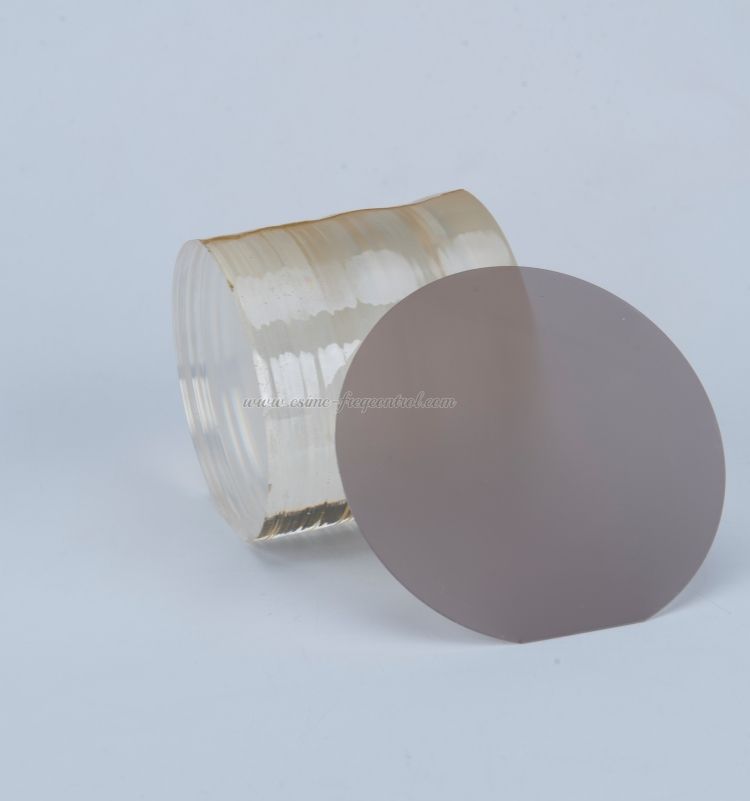
A lithium tantalate wafer is a thin, polished slice of lithium tantalate crystal, commonly written as LiTaO3. It is a ferroelectric and piezoelectric material. In a SAW device, an interdigital transducer (IDT) applies an alternating voltage to the wafer surface. The piezoelectric effect changes this electrical energy into a mechanical wave that travels along the surface. A receiving IDT then converts the wave back into an electrical signal.
The wafer is normally cut from a single crystal and supplied with a defined crystallographic orientation, thickness, diameter, surface roughness, and polishing grade. These specifications control the acoustic velocity, electromechanical coupling, frequency response, and production yield of the final device.
SAW filters are used when a compact circuit must select or reject radio-frequency signals. Mobile phones, wireless infrastructure, GNSS receivers, automotive systems, industrial sensors, and Internet of Things devices all use frequency-selective components.
Lithium tantalate is important because it combines piezoelectric activity with a stable single-crystal structure. Published material data commonly place the Curie temperature of lithium tantalate near 600°C, although the exact value depends on crystal composition and measurement conditions. This temperature is far above the operating temperature of most commercial RF modules, but it should not be treated as a guarantee of unlimited thermal reliability.
For a SAW filter, the useful performance depends on more than the Curie temperature. The design team must also control:
SAW filters based on lithium tantalate are used to separate desired frequency bands from unwanted signals. In a wireless front end, the filter must maintain its center frequency, insertion loss, bandwidth, and rejection over temperature and production variation.
Applications include:
A SAW resonator uses acoustic resonance to provide a stable frequency reference. The wafer cut, electrode pitch, and acoustic path determine the resonant frequency. A clean surface and uniform crystal are important because local defects can increase frequency spread between devices.
Lithium tantalate is also used in piezoelectric sensing structures. A change in mass, temperature, or surface condition can shift the acoustic response. The sensing layer, electrode material, and packaging must be selected together because moisture and contamination may create a signal that is larger than the target measurement.
Lithium tantalate has pyroelectric properties, meaning that a temperature change can produce a measurable electrical signal. This makes it useful in selected infrared detectors and thermal sensing systems. These products may require different wafer cuts and surface treatments from standard SAW filters.
| Advantage | Engineering value | What to verify |
|---|---|---|
| Piezoelectric response | Supports electrical-to-acoustic signal conversion in SAW devices. | Crystal cut, propagation direction, coupling coefficient, and device frequency. |
| Single-crystal uniformity | Reduces device-to-device frequency variation when wafer quality is controlled. | Defect density, inclusions, thickness uniformity, and surface inspection results. |
| High thermal margin | Provides a large material margin between normal module temperatures and the Curie transition. | Actual operating temperature, thermal cycling, TCF, and package stress. |
| Thin-wafer process compatibility | Allows photolithography, metal deposition, dicing, and wafer-level assembly. | Diameter, thickness, bow, warp, edge exclusion, and polishing quality. |
These advantages do not remove the need for process control. A wafer with the wrong orientation or uncontrolled surface damage can produce a device that fails even when the material name is correct.
Crystal orientation changes acoustic velocity, coupling, temperature behavior, and spurious-mode response. Common SAW designs may use orientations described by notation such as 36° YX, but the correct cut depends on the filter architecture and target band.
Do not order a wafer by diameter alone. The purchase specification should state the cut, propagation direction, thickness, tolerance, and intended application. If the design team changes the cut without updating the electrode layout, the center frequency and bandwidth may move outside the target range.
The IDT is fabricated on or near the wafer surface. Scratches, pits, particles, and polishing damage can cause electrode breaks, acoustic scattering, and local electrical leakage. The supplier should provide a surface inspection method and acceptance limit, such as inspection under a defined magnification and lighting condition.
Atomic force microscopy or optical profilometry may be used when the device requires tighter roughness control. A single roughness number is not enough. Inspection should also record defect size, defect density, location, and edge exclusion.
Thickness variation affects wafer handling and can influence acoustic and packaging behavior. Bow and warp can reduce lithography focus margin, create nonuniform bonding pressure, and increase the risk of wafer breakage.
Incoming inspection should measure thickness at multiple points rather than at the center only. A useful inspection record includes:
SAW devices experience frequency changes as temperature changes. The temperature coefficient of frequency depends on the crystal cut, electrode structure, passivation, and package stress. A device may pass room-temperature testing but fail at the low or high end of its operating range.
Qualification should measure center frequency, insertion loss, bandwidth, and rejection before and after temperature cycling. The test temperature range must match the product requirement. Automotive and outdoor products generally require a wider temperature range than indoor consumer electronics.
Lithium tantalate itself is not the only reliability concern. Moisture, ionic contamination, adhesive outgassing, and package leakage can affect the electrode and acoustic surface. A hermetic or controlled package may be required for products exposed to humidity, vibration, or temperature changes.
Use moisture-sensitive handling procedures when the package or electrode stack requires them. Cleanroom controls should define particle limits, wafer storage time, protective films, and cleaning chemicals. A suitable wafer can still produce poor field reliability if the assembly environment is uncontrolled.
Aluminum is common in SAW electrode structures, but the exact metal stack depends on power, frequency, fabrication process, and reliability requirements. Metal thickness, adhesion, grain structure, and electromigration resistance should be evaluated with the wafer material.
High RF power can produce localized heating at the IDT. The design should check power density, duty cycle, thermal path, and electrode aging. A wafer’s high Curie temperature does not mean the metal electrode can operate without thermal limits.
Start with the final device rather than the supplier catalog. Record the following information:
Ask the material supplier or device designer to confirm the crystal cut and propagation direction. The wafer orientation should be linked to the acoustic simulation and mask design. Confirm whether the supplier uses optical, X-ray, or another method to verify orientation.
A professional specification should include diameter, thickness, tolerance, orientation, surface finish, roughness, flatness, resistivity if relevant, edge profile, packaging, and inspection method. It should also define acceptable scratches, particles, chips, cracks, and inclusions.
Request a sample lot before placing a volume order. The certificate of analysis should identify the material grade, crystal orientation, wafer dimensions, inspection results, and lot number. Sample testing should use the same cleaning and lithography process planned for production.
Wafer-level inspection cannot replace a functional device test. Build test structures or a small pilot lot and measure:
After the pilot lot passes, establish a controlled purchase specification. Include change-notification requirements. A change in crystal growth, polishing slurry, cleaning method, packaging material, or inspection equipment may affect the final device.
For companies comparing lithium tantalate wafer suppliers, the most useful comparison is not price alone. Compare lot consistency, inspection evidence, technical support, sample-to-volume matching, delivery performance, and documented change control.
| Problem | Possible cause | Recommended action |
|---|---|---|
| Center frequency is outside specification | Wrong crystal cut, electrode pitch error, thickness variation, or temperature mismatch. | Verify wafer orientation, mask dimensions, thickness map, and test temperature. |
| High insertion loss | Surface roughness, particles, weak electrode adhesion, acoustic scattering, or package loss. | Review wafer inspection data, cleanroom records, electrode deposition, and package design. |
| Large frequency spread across one wafer | Nonuniform thickness, crystal defects, lithography variation, or thermal gradients. | Map wafer thickness and device frequency by position; compare with defect locations. |
| Cracks during dicing | Edge chips, excessive mechanical stress, unsuitable blade, or incorrect feed speed. | Inspect wafer edges, optimize dicing parameters, and use a qualified protective film. |
| Performance changes after humidity testing | Package leakage, contamination, electrode corrosion, or moisture-sensitive materials. | Check package sealing, ionic cleanliness, metal stack, and moisture test records. |
Before accepting a wafer lot, use a documented incoming inspection plan. The following checklist covers the most important controls:
Engineers should use peer-reviewed research and recognized technical organizations when selecting material data. The following resources provide useful background:
When using a technical reference, check the crystal composition, wafer cut, frequency range, temperature range, and test method. Data from one orientation or electrode structure should not be copied directly to a different design.
The main use is the fabrication of piezoelectric devices, especially SAW filters and resonators. It is also used in selected sensors, pyroelectric detectors, and other acoustic components.
No. The best substrate depends on frequency, bandwidth, coupling, temperature behavior, power handling, cost, and package requirements. Lithium tantalate may provide useful piezoelectric performance, but quartz, lithium niobate, and other materials may be better for specific designs.
The orientation should come from the acoustic design. A common orientation may be suitable for one filter architecture but unsuitable for another. Confirm the cut and propagation direction with simulation, supplier data, and test structures.
Thickness affects mechanical handling, flatness, processing yield, and interactions between the acoustic wave and the substrate. The exact influence depends on the device structure and frequency. Thickness should therefore be specified with a tolerance and measured across the wafer.
Lithium tantalate has a Curie temperature near 600°C in commonly cited material data, but the complete SAW device usually has a much lower practical limit. Electrodes, passivation, package materials, adhesives, and frequency drift must all be evaluated.
Ask for the crystal orientation, diameter, thickness, TTV, bow, warp, surface inspection results, roughness data when applicable, edge condition, lot traceability, and packaging information. A certificate should clearly identify the inspection method and acceptance limits.
Control edge chips, wafer mounting, blade condition, feed speed, spindle speed, cooling, and protective film selection. A small dicing trial should be completed before volume processing, especially for thin wafers.
Contact a qualified supplier such as CQT with your target frequency, crystal cut, wafer size, thickness, surface requirements, operating temperature, and annual volume. Providing these details allows the supplier to recommend a specification instead of offering a generic wafer.
Begin by preparing a one-page device requirement sheet. Include the target frequency, bandwidth, temperature range, power level, wafer size, crystal orientation, processing flow, and reliability tests. Then request a sample lot, review the certificate data, fabricate test structures, and compare the measured results with the production target.
For further understanding or a trial order, discuss the application with CQT and ask for a wafer specification, sample availability, inspection report, and recommended handling guide. Careful control of orientation, surface condition, dimensions, packaging, and qualification testing will give high-temperature lithium tantalate wafers a better chance of delivering stable SAW performance from the first engineering lot through volume production.


Copyright © Hangzhou Freqcontrol
Electronic Technology Ltd.
All Rights Reserved | Sitemap |
Powered by 







 中文


