Cost and Yield Considerations When Comparing Piezoelectric Wafer Materials means evaluating not only the purchase price of a wafer, but also its usable yield, processing losses, inspection requirements, device performance, and total manufacturing cost. In practical terms, CQT can help engineering and procurement teams compare materials such as Lithium Niobate Wafers, quartz, lithium tantalate, PZT, and aluminum nitride before committing to production. This approach protects business margins because a wafer with a higher unit price may deliver a lower cost per qualified device when it offers better uniformity, fewer defects, and a higher assembly yield.
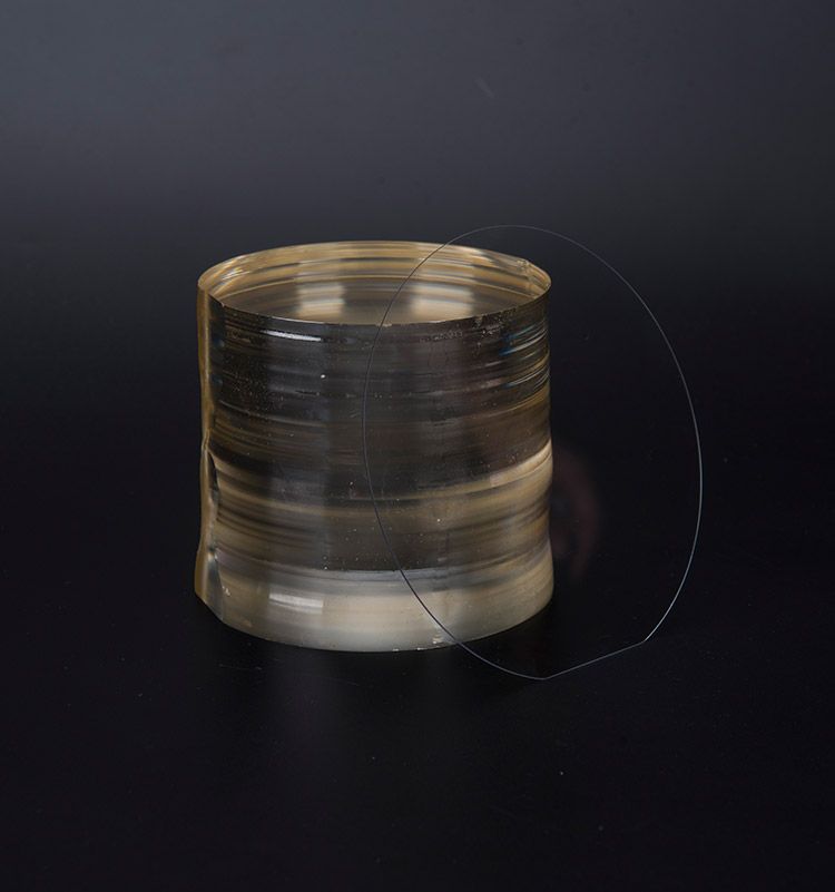
Piezoelectric wafers convert mechanical stress into electrical charge and can also deform when an electric field is applied. This property supports filters, resonators, acoustic sensors, ultrasonic transducers, microelectromechanical systems (MEMS), optical modulators, and radio-frequency components.
However, material selection affects much more than electromechanical coupling. It influences:
For CQT, the correct commercial question is therefore not “Which wafer is cheapest?” It is “Which material produces the lowest cost per accepted device at the required performance level?”
Quartz was one of the earliest widely adopted piezoelectric materials because of its stable resonant behavior, low aging rate, and established frequency-control applications. As demand expanded for higher coupling, acoustic power handling, optical integration, and miniaturized electronics, manufacturers adopted additional materials.
| Material | Typical strengths | Primary cost and yield concerns | Common applications |
|---|---|---|---|
| Quartz | Excellent frequency stability, mature processing, low aging | Orientation control, lower coupling than some engineered ceramics, machining sensitivity | Timing devices, resonators, sensors |
| Lithium Niobate | Strong piezoelectric response, high electromechanical coupling, optical and RF functionality | Material price, brittle handling, crystal quality, wafer bow, surface damage | SAW filters, optical modulators, acoustic sensors |
| Lithium Tantalate | Good temperature behavior and acoustic performance | Substrate availability, dicing and polishing losses, orientation requirements | RF filters, resonators, pyroelectric devices |
| PZT ceramics | High piezoelectric coefficients and strong actuation | Wafer uniformity, lead-containing process controls, electrode and sintering variation | Actuators, ultrasonic transducers, energy harvesting |
| Aluminum Nitride | CMOS-compatible potential, high thermal conductivity, lead-free composition | Film stress, texture, deposition rate, crystal orientation, defect density | MEMS, RF filters, acoustic resonators |
This history explains why there is no universal “best” piezoelectric wafer. Each material represents a trade-off between electrical performance, manufacturability, supply-chain risk, and qualification cost.
A reliable comparison should separate direct wafer cost from conversion cost. Direct wafer cost includes the substrate, orientation, diameter, thickness, grade, and inspection package. Conversion cost includes cleaning, coating, lithography, etching, metallization, dicing, testing, and scrap.
A basic calculation is:
Cost per good wafer = wafer purchase cost ÷ incoming acceptance yield
For example, assume two substrates:
The effective substrate cost is approximately $105.26 for Material A and $146.46 for Material B. Material A remains less expensive at the incoming stage. However, if Material A produces only 70% good devices after processing while Material B produces 90%, the cost per accepted device can reverse once fabrication and test costs are included.
Wafer diameter alone does not determine productivity. Usable area is reduced by edge exclusion, exclusion zones around defects, kerf loss, street width, and die layout. A supplier should provide:
For high-volume production, a 0.5 mm improvement in edge exclusion or a reduction in dicing chipping can create more economic value than a small reduction in the quoted wafer price.
Piezoelectric wafer yield is influenced by several parameters:
For precision manufacturing, acceptance criteria should be measurable. A project specification may require thickness accuracy to 0.01 mm, particle inspection across 100% of the wafer surface, and a documented nonconformance report for every rejected lot. These requirements should be agreed before sampling rather than added after delivery.
Lithium Niobate Wafers are attractive when high electromechanical coupling, surface acoustic wave performance, or electro-optic functionality is important. Their value is especially clear in RF filters, acoustic-wave devices, and integrated photonics.
Nevertheless, Lithium Niobate Wafers can require stricter control of crystal orientation, wafer handling, polishing, and thermal processing. The material is relatively brittle, and surface damage or microcracks may become yield limiters during dicing. A lower-cost quartz or AlN option may be more economical when the design does not require lithium niobate’s coupling or optical properties.
CQT buyers should compare the following technical parameters rather than relying on material names alone:
| Evaluation item | Why it affects cost | Recommended evidence |
|---|---|---|
| Cut and orientation | Changes mode frequency, coupling, and device sensitivity | Orientation certificate and X-ray diffraction data where applicable |
| Surface finish | Impacts bonding, metallization, and defect-related scrap | AFM or profilometry report; roughness target such as Ra in nanometers |
| Thickness and TTV | Controls frequency distribution and process uniformity | Mapping data from multiple points across each wafer |
| Piezoelectric response | Determines device output and design margin | dij, k2, dielectric constant, and loss tangent data |
| Mechanical integrity | Predicts chipping, cracking, and dicing yield | Visual inspection, microscope images, and lot-level breakage records |
Quality claims are meaningful only when the test method, sampling plan, and measurement uncertainty are clear. CQT and its customers should define the applicable standard for each characteristic instead of using a generic “qualified” label.
Useful references may include:
For Lithium Niobate Wafers, quartz, and other crystalline substrates, many dimensional and optical requirements are customer-specific. Therefore, the purchase specification should state gauge resolution, sampling frequency, calibration status, inspection coverage, and lot traceability. A robust supplier can provide a certificate of analysis, wafer map, visual inspection record, and response to a quality inquiry within 24 hours.
This is one of the most frequent errors. A low-price wafer can create higher costs through additional cleaning, rework, alignment correction, scrap, and customer returns. Always calculate cost per accepted die.
Piezoelectric coefficient is important, but yield also depends on wafer flatness, electrode design, thermal expansion, dielectric loss, crystal quality, and process compatibility. A material with excellent coupling may still perform poorly if it cannot meet the line’s bonding or dicing requirements.
100% inspection means every specified unit or surface area is examined using a defined method. It does not mean that every defect is detectable. Inspection capability, resolution, false-reject rate, and operator or equipment repeatability must be documented.
Grade, cut, orientation, thickness, polish, dopant level, thermal history, and supplier process can produce major differences. Two Lithium Niobate Wafers from different sources may have different propagation loss, surface quality, and dicing behavior.
Consider a CQT customer developing a 10 mm × 5 mm acoustic device. Supplier X offers a lower-cost wafer, but pilot data shows:
Supplier Y offers Lithium Niobate Wafers at a higher unit price, with:
Even if Supplier Y’s wafer price is 30% higher, the number of accepted devices per purchased wafer may be substantially greater. The correct decision should be based on a controlled pilot lot, including process time, dicing loss, electrical test distribution, and field-reliability data.
Cost and Yield Considerations When Comparing Piezoelectric Wafer Materials should focus on cost per good device, not the initial quotation alone. For CQT projects, the strongest evaluation combines material performance, wafer geometry, surface condition, process compatibility, inspection evidence, and supply continuity.
Lithium Niobate Wafers can justify a higher purchase price when their coupling, acoustic, RF, or electro-optic performance improves device yield and product value. Quartz, lithium tantalate, PZT, and AlN may be more suitable when their processing advantages outweigh the benefits of lithium niobate.
By using a documented specification, recognized testing methods such as applicable ASTM, IEC, IEEE, or ISO standards, and a pilot-lot yield model, CQT customers can reduce qualification risk and make a defensible sourcing decision. The next step is to request comparable wafer data and calculate the expected cost per accepted device before selecting the production material.


Copyright © Hangzhou Freqcontrol
Electronic Technology Ltd.
All Rights Reserved | Sitemap |
Powered by 







 中文


