Single Crystal Quartz Wafers support precise work in semiconductor processing, sensors, optics, and frequency-control devices. Unlike ordinary glass, quartz wafers have an ordered crystal lattice and useful piezoelectric behavior. Buyers comparing custom single crystal quartz wafers, high-purity quartz wafers, and single crystal quartz wafer suppliers must check crystal orientation, thickness tolerance, surface finish, purity, and delivery inspection data. These details affect device yield, signal stability, thermal performance, and long-term reliability.
Quartz wafers are used when a process needs electrical insulation, low contamination, chemical resistance, or controlled mechanical and acoustic behavior. The right wafer is not simply the clearest or thickest option. It must match the process temperature, wavelength, frequency, electrode design, and equipment geometry.
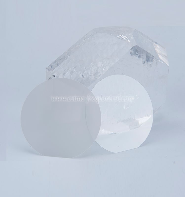
A single crystal quartz wafer is a thin, polished section cut from one continuous quartz crystal. Its atoms follow one regular lattice direction across the wafer. This structure gives the material stable mechanical, optical, electrical, and thermal properties.
The most common material is crystalline silicon dioxide, written as SiO2. Natural quartz can contain inclusions and trace elements, so electronic and sensor applications often use hydrothermal synthetic quartz. Synthetic growth provides better control over purity, crystal defects, dimensions, and orientation.
Single crystal quartz should not be confused with fused silica. Fused silica is an amorphous form of SiO2; it has no long-range crystal lattice and does not provide the same anisotropic piezoelectric response. The correct material depends on the application.
Quartz has a combination of properties that is difficult to obtain in one material:
The U.S. Geological Survey identifies quartz as a major industrial mineral used in electronics, glass, foundry work, and other manufacturing sectors. The IEEE piezoelectricity standard also provides the technical framework used to describe piezoelectric materials and their constants. These references show why quartz selection must be linked to measurable material and device requirements rather than appearance alone.
Sources: and .
Quartz crystal resonators and oscillators use the piezoelectric effect to create a stable mechanical resonance. The resonant frequency is influenced by crystal cut, thickness, electrode mass, dimensions, mounting stress, and temperature.
For this reason, a wafer manufacturer may need to control orientation within a defined angular tolerance and supply a narrow thickness range. A small dimensional change can shift the target frequency. In production, the customer should request frequency or cut-angle data when the wafer will be processed into resonators.
Surface acoustic wave devices use electrodes to launch and detect waves that travel along the wafer surface. These devices are used in filters, wireless communication systems, identification tags, sensors, and signal-processing modules.
Surface roughness and crystal orientation are especially important. Roughness can increase acoustic loss, while an incorrect cut can change wave velocity, coupling, and temperature response. The electrode material and deposition process must also be compatible with the quartz surface.
Quartz wafers can serve as insulating substrates, carrier wafers, process support wafers, or test platforms. Their low electrical conductivity is useful when a process must reduce parasitic current or isolate a thin film from the substrate.
Before using quartz in a cleanroom, ask for cleaning specifications, particle limits, metallic contamination data, packaging conditions, and lot traceability. A wafer may meet its diameter and thickness specifications but still fail a high-sensitivity process because of particles or trace metals.
Polished quartz substrates are used for windows, optical test parts, photomasks, ultraviolet components, and spectroscopy equipment. The required grade depends on the operating wavelength. Deep-ultraviolet work generally needs tighter control of absorption, inclusions, bubbles, striae, and polishing defects than visible-light applications.
Request a transmission curve or absorption specification instead of relying on the phrase “optical grade.” A useful specification states the wavelength range, sample thickness, measurement method, and acceptable transmission level.
Quartz crystal microbalances measure changes in resonance frequency caused by added mass on a coated surface. The Sauerbrey equation is commonly used for a rigid, thin, evenly distributed film:
Δm = −Cf × Δf / n
Here, Δm is the mass change per unit area, Δf is the frequency shift, n is the overtone number, and Cf is the mass sensitivity constant. The equation becomes less reliable for soft, liquid, rough, or viscoelastic films. A 2001 review in Journal of Chromatography A explains the use and limitations of quartz crystal microbalance methods in chemical analysis.
Source: .
A purchasing specification should convert the process requirement into measurable limits. The following items should appear on the quotation or technical data sheet.
| Specification | Why it matters | Questions to ask the supplier |
|---|---|---|
| Diameter and shape | Determines equipment compatibility and usable area. | What are the nominal diameter, edge exclusion, notch or flat design, and diameter tolerance? |
| Thickness | Controls resonance, optical path length, stiffness, and handling strength. | What are the nominal thickness and upper and lower limits? |
| TTV, bow, and warp | Influence bonding, lithography focus, coating uniformity, and wafer handling. | Where are measurements taken, and which instrument and sampling plan are used? |
| Crystal orientation | Affects piezoelectric coupling, acoustic velocity, thermal behavior, and optical response. | Is orientation verified by X-ray diffraction? What is the angular tolerance? |
| Surface finish | Influences film adhesion, scattering, electrode patterning, and bonding. | Is the wafer single-side or double-side polished? What are Ra, scratches, digs, and haze limits? |
| Material purity | Impurities can change optical absorption, electrical behavior, and cleanroom yield. | Which trace elements are controlled, and is a certificate of analysis available? |
| Edge quality | Chips and sharp edges can create particles or cause wafer breakage. | Are edge rounding, chamfer size, and edge-chip limits defined? |
| Cleaning and packaging | Protects the wafer from particles, organic residue, and handling damage. | What cleaning process, packaging class, and lot identification are supplied? |
Commercial quartz wafers may be produced in sizes such as 2, 3, 4, 6, or 8 inches, but availability depends on crystal growth, thickness, cut, and production volume. A supplier may also offer custom diameters for research or sensor assemblies.
Do not compare two quotations only by nominal size. A “100 mm wafer” can have different usable areas if the edge exclusion, flatness, notch, and edge profile are different. Likewise, “polished” does not state whether the surface is suitable for optical work, thin-film deposition, or direct bonding.
Each stage can affect yield. For example, excessive grinding damage may remain beneath the polished surface, while poor edge handling may create chips during shipping. Ask whether the supplier provides process control records or only a final visual inspection.
Start with a one-page technical request. Include the diameter, thickness, crystal cut, orientation tolerance, polishing method, roughness target, TTV, edge profile, purity level, quantity, and intended application.
Then use this supplier-check process:
CQT can be considered when you need quartz crystal materials, frequency-control components, or application-specific technical support. Before placing a volume order, request current specifications, sample inspection results, and written confirmation of the acceptance criteria.
Possible causes include excessive thickness variation, sharp edges, hidden saw damage, thermal shock, or unsuitable vacuum handling. Check edge chamfer dimensions, wafer flatness, handling temperature, and packaging protection. A thicker wafer may improve handling, but it can also change resonance or optical performance, so the solution must match the application.
Possible causes include organic residue, high surface roughness, moisture, poor activation, or an incompatible coating process. Compare single-side and double-side polished samples, confirm the cleaning recipe, and measure contact angle or surface energy when appropriate.
Check thickness distribution, crystal cut angle, electrode mass, electrode area, mounting stress, and temperature. The wafer thickness alone may not explain the result. For production work, ask for orientation tolerance and thickness mapping rather than one center-point measurement.
Confirm the test wavelength and wafer thickness. Inspect for inclusions, haze, scratches, coating absorption, and contamination. “Transparent quartz” is not a complete optical specification; the supplier should provide measured transmission or absorption data for the required wavelength range.
No. Single crystal quartz has an ordered crystal lattice and anisotropic piezoelectric properties. Quartz glass, often referring to fused silica, is amorphous. They may share chemical composition but behave differently in acoustic, optical, thermal, and electrical applications.
The correct cut depends on the application. Frequency devices may require AT-cut, BT-cut, or another defined orientation. Optical, sensor, and substrate applications may use a different cut or surface direction. Ask the supplier to connect the cut recommendation to frequency, temperature range, wave mode, or optical requirement.
There is no single value for every process. A research substrate, optical window, thin-film electrode base, and bonding wafer can require different roughness limits. Specify Ra or RMS, measurement length, instrument type, and whether the requirement applies to one or both surfaces.
Quartz has a high melting point, but the practical limit is lower than the melting point in many processes. Thermal gradients, wafer thickness, mounting stress, coatings, and repeated heating cycles can cause cracking or distortion. Test the complete wafer-and-fixture assembly at the intended temperature.
Use controlled cleaning, sealed packaging, proper wafer tweezers or vacuum tools, and a defined inspection method. Also check edge chipping because particles often come from damaged edges. Request particle limits and packaging details in the purchase specification.
Standard wafers usually offer shorter lead times and lower development cost. Custom wafers are useful when the device requires a special diameter, cut angle, thickness, edge shape, coating, or surface finish. Test a standard sample first if it can represent the final process.
Define the application first, then create a specification sheet with dimensions, crystal orientation, flatness, surface finish, purity, cleaning, packaging, and inspection requirements. Read the supplier’s user guide and handling instructions before processing the sample. If you are comparing custom single crystal quartz wafers, high-purity quartz wafers, or single crystal quartz wafer suppliers, ask CQT for a technical review and sample plan. This approach reduces specification gaps, prevents avoidable breakage, and gives your production team measurable acceptance criteria.


Copyright © Hangzhou Freqcontrol
Electronic Technology Ltd.
All Rights Reserved | Sitemap |
Powered by 







 中文
中文


