Lithium Tantalate Wafers are engineered crystal substrates used in surface acoustic wave (SAW) filters, RF duplexers, resonators, sensors, and optical devices. As wireless systems move from 5G to higher-frequency networks, component makers need materials that combine stable piezoelectric behavior, low electrical loss, and reliable wafer processing. This guide explains how lithium tantalate wafers for SAW filters work, how they compare with other materials, and how to select a supplier for high-volume RF production.
Modern mobile devices must separate transmit and receive signals inside a small space. A phone may support several cellular bands, Wi-Fi standards, Bluetooth, and satellite positioning at the same time. This creates three main engineering problems:
Lithium tantalate, commonly written as LiTaO3, is a ferroelectric and piezoelectric single-crystal material. Its piezoelectric effect converts an electrical signal into a mechanical surface wave and then converts that wave back into an electrical signal. This makes it suitable for compact acoustic filters and resonators.
Unlike a simple conductor, a piezoelectric wafer creates a controlled mechanical response at a specific frequency. Interdigital transducers, or IDTs, are patterned on the wafer surface. The width and spacing of the metal fingers determine the acoustic wavelength and therefore the operating frequency.
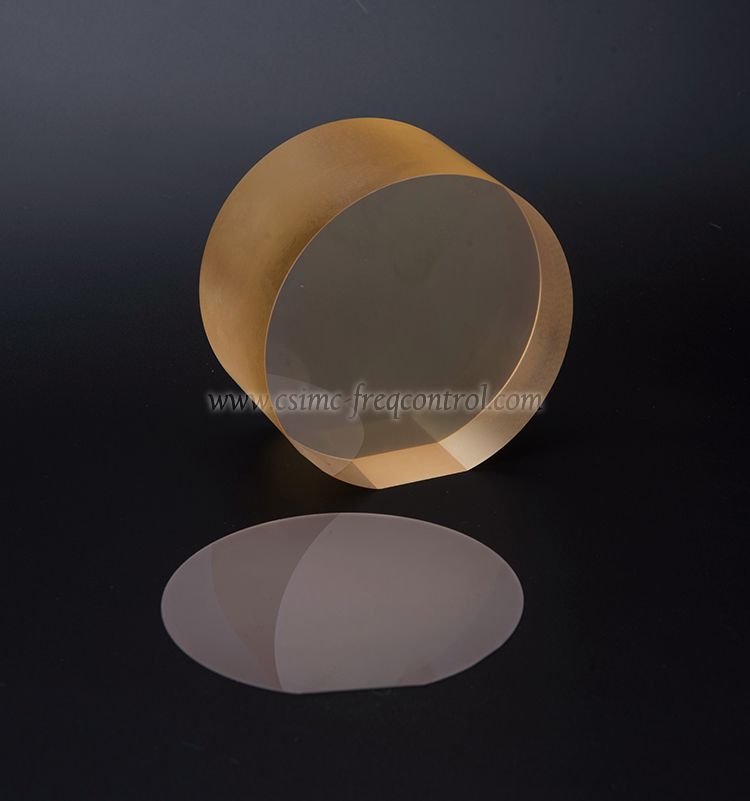
Lithium tantalate wafers are thin, polished slices cut from a lithium tantalate single crystal. They are supplied in different diameters, thicknesses, crystal orientations, and surface finishes for specific device designs.
| Term | Meaning | Why it matters |
|---|---|---|
| LiTaO3 | Chemical formula for lithium tantalate | Identifies the crystal material used for the substrate |
| Piezoelectricity | Conversion between mechanical strain and electrical charge | Allows acoustic wave generation and detection |
| SAW | Surface acoustic wave | Provides frequency-selective filtering on the wafer surface |
| Crystal orientation | Cut direction, such as X-cut or rotated Y-cut | Changes coupling, temperature behavior, and wave propagation |
| Electromechanical coupling coefficient | A measure of how efficiently electrical energy couples to mechanical motion | Higher coupling can support wider filter bandwidth, depending on the design |
| TTV | Total thickness variation across a wafer | Low TTV improves lithography, bonding, and device consistency |
| Ra | Average surface roughness | A smoother surface supports accurate thin-film and electrode processing |
Material selection cannot be based on coupling alone. Designers also evaluate acoustic velocity, dielectric loss, temperature coefficient of frequency, power handling, wafer strength, surface quality, and compatibility with the manufacturing line.
A basic SAW filter contains a piezoelectric substrate and two or more IDTs. The input IDT receives an RF signal and creates a surface acoustic wave. The wave travels across the crystal surface. The output IDT detects the wave and changes it back into an electrical signal.
The approximate center frequency depends on acoustic velocity and electrode pitch:
f ≈ v / λ
Here, f is frequency, v is acoustic velocity, and λ is acoustic wavelength. Smaller electrode features allow higher operating frequencies, but they also increase the need for accurate lithography, clean surfaces, and tight wafer uniformity.
For this reason, an RF wafer supplier must control both the crystal and the finished surface. A wafer with good bulk properties but poor flatness or contamination can still cause low yield during electrode fabrication.
Different RF applications need different material characteristics. Lithium tantalate is one option within a broader family of piezoelectric and acoustic materials.
| Material | Typical strengths | Design considerations | Common applications |
|---|---|---|---|
| Lithium tantalate | Strong piezoelectric response, useful RF filtering behavior, good optical and pyroelectric performance | Crystal orientation, thermal behavior, electrode design, and wafer quality must be controlled | SAW filters, resonators, RF modules, sensors, optical components |
| Lithium niobate | High piezoelectric response and strong electro-optic performance | Temperature stability and power-handling requirements depend on the cut and device structure | Acoustic devices, optical modulators, frequency control, photonics |
| Quartz | Excellent frequency stability and low temperature sensitivity in selected cuts | Lower coupling can require different device geometry and process design | Timing components, oscillators, stable frequency references |
| AlN | Wide bandgap, strong thermal performance, and compatibility with thin-film processing | Thin-film stress, deposition quality, and electrode integration affect performance | BAW filters, MEMS, sensors, high-frequency devices |
| ScAlN | Enhanced piezoelectric response compared with conventional AlN in many compositions | Scandium content, film uniformity, stress, and process stability require close control | Advanced BAW and MEMS devices |
The right choice depends on the device architecture. A SAW filter designer may prioritize coupling and surface quality, while a timing-device designer may place greater weight on temperature stability. A direct material comparison without the target frequency, bandwidth, power level, and packaging method can lead to the wrong substrate decision.
SAW filters made on lithium tantalate substrates can be used in RF front-end circuits to separate frequency bands. These filters support functions such as band selection, duplexing, and interference rejection in wireless products.
Engineers normally review:
Piezoelectric resonators use the mechanical vibration of the crystal to create a frequency-selective response. The resonator geometry, crystal cut, electrode material, and packaging all affect the final quality factor and frequency stability.
SAW devices can operate as passive or remotely interrogated sensors. Changes in temperature, pressure, strain, or surface chemistry can shift the acoustic response. This makes them useful in industrial equipment, battery monitoring, environmental sensing, and asset tracking.
Lithium tantalate also has electro-optic and nonlinear optical properties. In selected designs, it can be used in optical modulation, frequency conversion, and integrated photonics research. The wafer specification for optical devices may differ from the specification for RF filters, especially in terms of domain control, optical loss, and surface polish.
Because lithium tantalate produces an electrical response when its temperature changes, it can be used in pyroelectric detectors. These devices may support infrared sensing and motion detection, although the required electrode structure and packaging differ from those used in SAW filters.
The piezoelectric response allows the filter function to be built directly into the substrate and electrode pattern. This supports small components with a controlled frequency response.
Different cuts and orientations can change acoustic propagation, coupling, and temperature response. This gives designers more options when balancing bandwidth, loss, and stability.
Lithium tantalate is not limited to one physical effect. Its piezoelectric, pyroelectric, electro-optic, and nonlinear optical properties support several device categories. This can be useful for manufacturers that need more than one type of crystal component.
RF device yield depends on wafer diameter, thickness, TTV, warp, bow, surface roughness, particle level, and edge quality. A controlled wafer process gives the lithography and electrode steps a more stable starting point.
However, the material is not automatically the best option for every product. The final decision should be based on measured device data rather than general claims. Important data includes S-parameters, frequency-temperature curves, power-aging results, and wafer inspection records.
A reliable supply chain usually includes the following steps:
High-purity raw materials are melted and formed into a single crystal. The growth method, stoichiometry, impurity level, and thermal history affect crystal quality. Optical and RF applications may require different defect and absorption limits.
The crystal is measured and cut according to the required orientation. The selected cut changes the piezoelectric constants and acoustic response. Orientation accuracy should be verified with suitable metrology rather than assumed from the nominal product name.
The boule is sliced into wafers using a precision cutting process. Saw damage, thickness variation, edge chipping, and subsurface damage must be controlled at this stage.
Wafer thickness is adjusted through lapping and polishing. Chemical-mechanical polishing may be used to reduce surface damage and improve roughness. The target specification should list thickness tolerance, TTV, warp, bow, and surface roughness.
Particles, metallic contamination, scratches, pits, and stains can reduce device yield. Inspection may include optical inspection, laser scanning, thickness mapping, crystal orientation testing, and surface roughness measurement.
For production use, the supplier should provide a certificate of analysis or certificate of conformity. Useful records include lot number, crystal orientation, wafer diameter, thickness, TTV, resistivity when relevant, surface finish, inspection results, and packaging conditions.
When comparing suppliers, use a technical checklist instead of comparing price alone.
| Evaluation area | Questions to ask |
|---|---|
| Material | What purity, composition, crystal-growth method, and defect limits are available? |
| Orientation | Can the supplier provide the required cut and orientation tolerance? |
| Wafer size | Are 2-inch, 3-inch, 4-inch, or larger formats available for the production line? |
| Thickness | What are the nominal thickness, tolerance, TTV, bow, and warp values? |
| Surface | Is the surface single-side polished or double-side polished? What are the Ra and defect limits? |
| Quality system | Are lot traceability, inspection reports, corrective actions, and change control available? |
| Technical support | Can the supplier help with sample evaluation, process matching, and failure analysis? |
Ask for sample wafers before approving a production order. Use the samples in the actual process flow and measure yield, electrode adhesion, frequency distribution, insertion loss, rejection, and temperature response. A wafer that performs well in a catalog specification may still require process adjustment in a particular fab.
A practical qualification plan should include both wafer-level and device-level tests.
For RF components, vector network analyzer measurements are commonly used to obtain S-parameters. These results show how much signal is reflected and transmitted across the frequency range. They provide more useful evidence than broad statements such as “high performance” or “excellent stability.”
The following technical sources can help engineers understand the material and its device applications:
When using published data, check the crystal cut, frequency range, temperature condition, electrode structure, and measurement method. Material values reported in one study cannot always be transferred directly to another wafer design.
Frequency variation may come from wafer thickness, crystal orientation, electrode dimensions, acoustic velocity, or temperature. Review wafer maps and device-level frequency distribution together to identify the main cause.
Low yield can result from particles, surface damage, poor edge quality, excessive TTV, or a mismatch between the wafer surface and the lithography process. Start with defect mapping instead of changing several process steps at once.
High loss may be caused by electrode resistance, acoustic scattering, surface roughness, package parasitics, or an unsuitable acoustic design. Wafer quality is important, but it is only one part of the loss budget.
SAW frequency changes with temperature because the acoustic velocity and dimensions of the device change. Crystal cut, electrode materials, temperature-compensation layers, and package design can all affect the final temperature coefficient.
Thin wafers are sensitive to edge chipping and mechanical stress. Use controlled wafer cassettes, clean handling tools, suitable edge exclusion, and packaging that protects the polished surface.
They are used for SAW filters, RF resonators, frequency-control devices, wireless sensors, pyroelectric detectors, and selected optical or electro-optic components.
No. Both are ferroelectric and piezoelectric crystals, but their acoustic, electrical, thermal, optical, and processing properties are different. The correct choice depends on the device frequency, bandwidth, temperature range, power, and manufacturing process.
Request the crystal orientation, diameter, thickness, thickness tolerance, TTV, bow, warp, surface roughness, polish type, edge specification, particle limits, defect limits, and lot documentation. For qualification, also request sample data from a production-equivalent lot.
They can support RF filtering functions used in many wireless systems, including components designed for 5G equipment. Actual suitability depends on the target band, bandwidth, power level, filter topology, packaging, and required insertion-loss and rejection values.
Wafer quality affects lithography, electrode pattern accuracy, surface scattering, bonding, and process yield. It does not determine the complete filter performance by itself. The electrode design, fabrication process, package, and circuit layout also matter.
Use a small, traceable lot and run it through the intended cleaning, coating, lithography, etching, electrode, dicing, and packaging steps. Compare yield and RF test results with the existing substrate. Record the results by wafer position to identify uniformity patterns.
CQT can be considered as a technical supplier or evaluation partner for lithium tantalate wafer projects. Before purchase, discuss the required crystal cut, wafer diameter, thickness, TTV, surface finish, inspection method, packaging, sample quantity, and production schedule with the CQT team.
Begin with the device requirements, not a generic wafer grade. Define the RF band, bandwidth, power, temperature range, package, wafer size, and process limits. Then request a technical datasheet, sample lot, inspection report, and application guidance from a qualified supplier. If you are developing a new filter or sensor, review the user guide and process recommendations before starting the trial. For an application-specific review, contact CQT with your target specifications and current material data; this is the practical next step for evaluating lithium tantalate wafers for RF components.


Copyright © Hangzhou Freqcontrol
Electronic Technology Ltd.
All Rights Reserved | Sitemap |
Powered by 







 中文
中文


