Key Selection Criteria for Lithium Tantalate Wafers in SAW Devices are the technical and commercial requirements used to choose a lithium tantalate (LiTaO3) substrate for surface acoustic wave applications. These criteria include crystal cut, orientation, wafer diameter, thickness, surface quality, temperature stability, electromechanical coupling, and inspection data. Selecting the correct Lithium Tantalate Wafers helps manufacturers improve SAW filter yield, frequency consistency, production reliability, and total business value.
For companies developing RF filters, duplexers, resonators, sensors, and timing components, the right wafer is not simply the lowest-cost wafer. A controlled substrate specification can reduce electrode-pattern variation, prevent frequency drift, shorten qualification cycles, and support stable mass production. CQT can be included in the supplier evaluation process as a technical partner for customized wafer requirements and quality documentation.
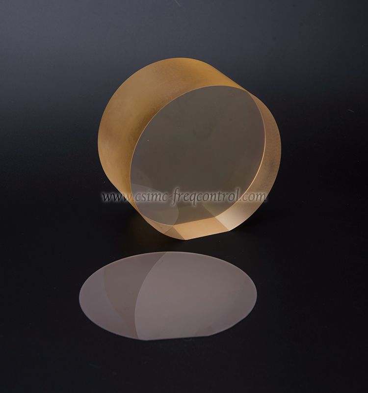
Lithium tantalate is a single-crystal ferroelectric material with strong piezoelectric properties. In a SAW device, an interdigital transducer, or IDT, converts an electrical signal into a surface acoustic wave. The wave travels along the wafer surface and is then converted back into an electrical signal.
LiTaO3 is widely used because it offers a useful combination of:
These characteristics have supported the growth of SAW technology in mobile communication, wireless infrastructure, automotive electronics, industrial sensing, and consumer devices. As operating frequencies increase and filter specifications become tighter, wafer quality becomes directly connected to device performance.
The crystal cut defines how the wafer is oriented relative to the crystallographic axes. It strongly affects the coupling coefficient, phase velocity, temperature coefficient of frequency, spurious response, and power-handling behavior.
The 36° YX-cut lithium tantalate wafer is commonly considered for SAW filter and resonator designs, but it is not suitable for every application. A device engineer may require another cut or propagation direction to achieve a specific balance between:
Before ordering, the purchase specification should state the cut, flat orientation, propagation direction, and allowable angular tolerance. A crystal label such as “LiTaO3 wafer” is not sufficiently detailed for production control.
Wafer diameter must match the lithography, metallization, bonding, and dicing equipment already installed in the factory. Common requirements may include 2-inch, 3-inch, 4-inch, or larger formats, depending on the production line.
Thickness influences acoustic behavior, mechanical strength, handling, and compatibility with wafer-level packaging. A practical purchase specification should identify:
For example, if a process requires an outside-diameter tolerance of ±0.01 mm, the supplier should confirm how the measurement is performed, which gauge is used, and whether the value applies before or after cleaning. Dimensional precision without a defined measurement method can create disputes during incoming inspection.
The polished surface must support uniform photolithography and stable metal deposition. Scratches, pits, haze, edge chips, particles, and polishing marks can cause open circuits, short circuits, electrode discontinuities, or local acoustic losses.
Important surface parameters include:
For high-frequency SAW devices, the required roughness may be in the nanometer range. However, the acceptable value depends on the electrode pitch, metal stack, resist process, and device frequency. The wafer supplier and device manufacturer should agree on the inspection area, scan method, instrument type, and reporting format.
Material properties determine how efficiently the wafer converts electrical energy into acoustic energy. A higher coupling coefficient can support wider bandwidth, but coupling alone does not guarantee a better filter. The final result also depends on IDT geometry, electrode material, metallization ratio, reflector design, and packaging.
Ask for available technical data related to:
Material data should be linked to the specific crystal cut and test direction. Values from one orientation should not automatically be applied to another orientation.
LiTaO3 is often selected for its useful piezoelectric performance, but SAW frequency still changes with temperature. This is important in automotive, outdoor wireless, industrial, and high-power RF environments.
When reviewing Lithium Tantalate Wafers, determine whether the application requires:
A wafer supplier cannot compensate for every system-level thermal effect. The package, electrode stack, bonding layer, and circuit architecture must also be included in the thermal design.
A detailed specification makes supplier comparison more reliable. The following checklist can be used when requesting a quotation from CQT or another qualified crystal-wafer manufacturer.
| Selection area | Information to specify | Why it matters |
|---|---|---|
| Material | LiTaO3 grade, single-crystal condition, dopant status if applicable | Controls electrical, acoustic, and thermal behavior |
| Crystal orientation | Cut angle, propagation direction, flat or notch direction | Determines velocity, coupling, TCF, and spurious modes |
| Geometry | Diameter, thickness, TTV, bow, warp, edge exclusion | Supports lithography, bonding, and wafer handling |
| Surface | Polish grade, Ra/RMS, scratches, pits, particles, haze | Reduces electrode and photolithography defects |
| Electrical properties | Resistivity or conductivity range, dielectric data where required | Supports the selected RF process and device architecture |
| Quality documents | Certificate of analysis, inspection report, lot traceability, packing record | Enables incoming inspection and failure analysis |
For production programs, buyers should request a representative sample lot before approving volume supply. A practical acceptance plan may include 100% visual inspection, dimensional sampling, surface inspection, and lot-based review of crystal orientation. If the application is highly sensitive, the contract should define the sampling level, rejection criteria, and corrective-action procedure.
Quality claims should be supported by measurable records rather than general statements such as “high precision” or “premium grade.” A supplier evaluation package may include:
The exact standard revision and test method should be written into the purchase order. ASTM, SEMI, DIN, and ISO references are useful only when the supplier identifies the applicable clause, measurement condition, and acceptance limit.
A low unit price may be offset by lower yield, additional cleaning, rework, or inconsistent device frequency. Total cost should include incoming inspection, process loss, engineering qualification, and delivery risk.
Different cuts can produce significantly different acoustic and thermal results. A wafer that works in one SAW filter design may fail to meet the bandwidth or TCF target in another design.
Lithium tantalate is a ferroelectric and pyroelectric material. Temperature changes and handling conditions can create electrical charge during processing. The fab may therefore need appropriate grounding, ionization, heating, and electrostatic-discharge controls.
A low Ra value does not prove that a wafer is clean or defect-free. Particle contamination, edge chips, and subsurface damage can still reduce yield. Surface morphology and cleanliness must be evaluated together.
A generic datasheet is not a substitute for a lot-specific certificate of analysis. Each production lot should be traceable to its crystal batch, orientation measurement, polishing process, inspection result, and packaging date.
Consider a hypothetical RF filter manufacturer experiencing unstable insertion loss and inconsistent center frequency across wafer lots. The initial purchase specification only stated “3-inch polished lithium tantalate wafer,” without identifying crystal angle, TTV, particle limits, or orientation tolerance.
The engineering team revised the specification as follows:
After the change, the manufacturer could separate wafer-related variation from lithography and electrode-process variation. The key lesson is not that one parameter solves every problem. Rather, a complete wafer specification gives the engineering team the data needed to control the full SAW manufacturing process.
When assessing CQT, buyers should use a structured qualification process instead of relying only on a product page or sample appearance.
Include the desired wafer diameter, thickness, crystal cut, orientation tolerance, polish grade, surface specification, quantity, packaging requirement, and intended SAW frequency range.
Check whether CQT clearly confirms available material grades, inspection capability, lead time, minimum order quantity, sample policy, and technical support. A professional response should identify any specification that requires clarification.
Inspect the sample wafers using the same equipment and criteria used for production incoming inspection. Where practical, process the samples through the actual photolithography, metallization, dicing, and device test flow.
Before volume ordering, agree on a control plan covering measurement frequency, calibration, lot release, nonconformance handling, change notification, and corrective action. This is especially important when the wafer is a custom cut or custom thickness.
The most important Key Selection Criteria for Lithium Tantalate Wafers in SAW Devices are crystal orientation, wafer geometry, surface finish, acoustic performance, temperature behavior, cleanliness, traceability, and supplier responsiveness. The best wafer is the one that matches the complete SAW process—not merely the one with the lowest purchase price.
By defining measurable requirements, requesting lot-specific evidence, referencing applicable SEMI, ASTM, DIN, or ISO methods, and validating samples in the real device process, manufacturers can reduce technical risk. CQT can be considered during this qualification process when its material capability, inspection records, delivery performance, and technical support meet the project requirements.
For a reliable sourcing decision, prepare a complete specification sheet and ask for a documented quotation, sample inspection plan, and certificate of analysis before beginning volume production.


Copyright © Hangzhou Freqcontrol
Electronic Technology Ltd.
All Rights Reserved | Sitemap |
Powered by 







 中文


