Application-Driven Material Comparison for Next-Generation RF Components is a method of selecting a substrate or functional material according to the component’s actual operating requirements—not simply choosing the material with the highest specification. For RF filters, resonators, duplexers, acoustic sensors, and electro-optic devices, this approach compares parameters such as electromechanical coupling, acoustic velocity, dielectric loss, thermal stability, wafer size, surface roughness, and manufacturing cost. For businesses, it reduces redesign risk, improves first-pass yield, and helps engineers select the right material for volume production.
For companies evaluating Lithium Niobate Wafers, CQT can serve as a technical reference point during supplier qualification and material selection. The correct choice depends on the frequency band, bandwidth, insertion loss, power handling, temperature range, packaging method, and production target of the RF component.
RF component development has moved from relatively narrowband communication systems to highly integrated platforms supporting 5G, 5G-Advanced, satellite communications, automotive radar, Wi-Fi, IoT, and aerospace electronics. These systems require tighter frequency control, lower insertion loss, wider bandwidth, higher power endurance, and better thermal management.
Historically, engineers often selected materials from a familiar material family. Quartz was widely valued for frequency stability, lithium tantalate for acoustic filtering, and silicon for semiconductor integration. As RF requirements became more demanding, however, material selection became a multi-variable engineering decision.
Application-Driven Material Comparison for Next-Generation RF Components addresses this change by connecting material properties to the complete device architecture. A material that performs well in a laboratory test may not be the most suitable option after considering electrode design, bonding, dicing, packaging, temperature compensation, and assembly yield.
Lithium niobate, commonly written as LiNbO3 or LN, is a ferroelectric crystal with strong piezoelectric, electro-optic, and nonlinear optical properties. In RF engineering, these characteristics make Lithium Niobate Wafers attractive for acoustic resonators, RF filters, tunable devices, integrated photonics, and high-frequency transducers.
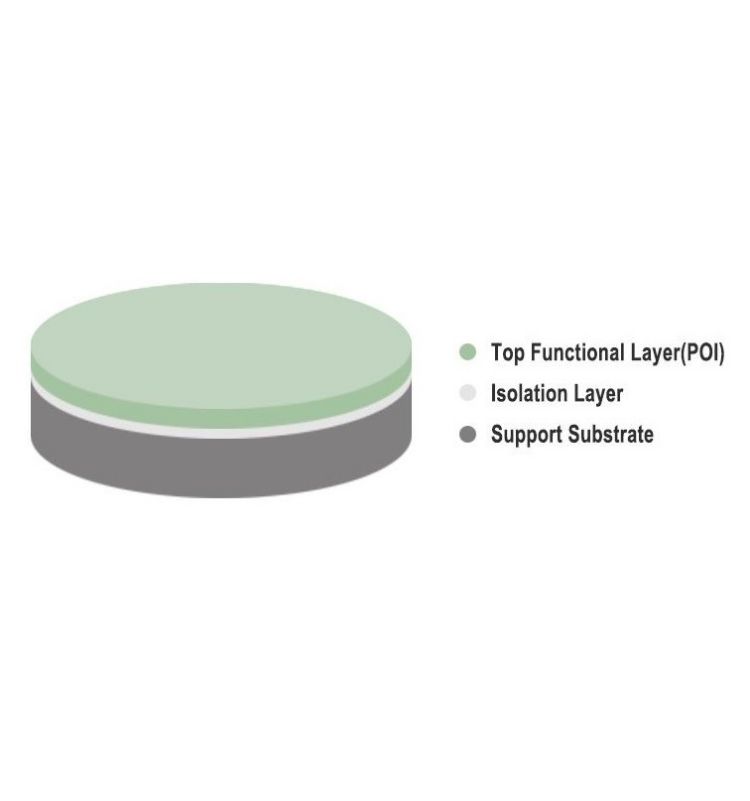
Thin-film lithium niobate, often called TFLN, has expanded the design space further. A thin LN layer bonded to a supporting substrate can provide strong acoustic or optical interaction while the handle wafer contributes mechanical stability and thermal management. This structure is useful when designers need high coupling, compact dimensions, and compatibility with advanced lithography.
Nevertheless, lithium niobate is not a universal replacement for every RF material. Its value must be assessed against the entire device process, including crystal cut, propagation direction, film thickness, electrode metal, bonding interface, thermal expansion, and packaging stress.
| Parameter | Why it matters | Typical material-selection question |
|---|---|---|
| Electromechanical coupling | Influences bandwidth and transduction efficiency | Can the material support the required filter bandwidth without excessive loss? |
| Acoustic velocity | Affects wavelength, resonator size, and operating frequency | Will the acoustic mode fit the target geometry and lithography limits? |
| Dielectric loss | Contributes to insertion loss and Q-factor degradation | Will the substrate maintain acceptable Q at the target frequency? |
| Thermal expansion | Changes frequency and creates package stress | Can the wafer and package maintain stability across the operating temperature range? |
| Surface condition | Controls lithography, bonding, and defect risk | Are roughness, particles, scratches, and crystal defects within process limits? |
The most useful comparison does not rank materials from “best” to “worst.” Instead, it identifies the best match for a specific component and manufacturing route.
| Material | Key strengths | Potential limitations | Relevant RF applications |
|---|---|---|---|
| Lithium niobate | High piezoelectric response, strong electro-optic effect, advanced thin-film integration | Thermal drift, bonding complexity, sensitivity to process and crystal orientation | Wideband filters, acoustic resonators, tunable RF devices, RF-photonic systems |
| Lithium tantalate | Good acoustic performance and temperature stability in selected designs | Different coupling and processing trade-offs compared with LN | SAW filters, resonators, frequency-control devices |
| Aluminum nitride | High thermal conductivity, strong electrical insulation, compatibility with thin-film processing | Coupling and bandwidth may differ from lithium niobate depending on orientation and structure | BAW resonators, RF filters, high-temperature devices |
| Quartz | Excellent frequency stability and mature supply chain | Lower electromechanical coupling in many configurations | Oscillators, timing references, narrowband frequency control |
| Silicon | Strong semiconductor ecosystem, high integration potential, scalable wafer processing | May require additional piezoelectric or insulating layers for acoustic functions | Integrated RF circuits, MEMS, hybrid acoustic systems |
| Gallium nitride | High-power and high-frequency semiconductor performance | Higher material and process complexity for certain passive RF functions | Power amplifiers, high-power RF front ends, microwave electronics |
This table illustrates why a lithium niobate wafer comparison should include the complete system objective. For example, a filter requiring wide bandwidth may benefit from LN’s high coupling, while a precision oscillator focused mainly on long-term stability may favor quartz.
When evaluating Lithium Niobate Wafers with CQT or another qualified supplier, the process should move from application requirements to measurable acceptance criteria. A structured workflow makes technical communication clearer and prevents costly assumptions.
Start with the device-level targets. Record the nominal frequency, bandwidth, Q-factor, insertion loss, power level, operating temperature, lifetime, and package configuration. Include the production forecast because a material that works for 100 prototypes may not be economical for 100,000 units per month.
For LN devices, the specification should identify whether the project requires bulk crystal or thin-film lithium niobate. It should also define crystal cut, orientation, film thickness, handle substrate, bonding structure, wafer diameter, and thickness tolerance.
Dimensional requirements should be unambiguous. For example, a drawing may call for a wafer thickness tolerance of ±0.01 mm, a defined edge-exclusion zone, and controlled bow and warp. These figures must be confirmed against the actual process capability rather than copied from a generic datasheet.
A professional qualification plan should cover more than visual appearance. Depending on the product, the incoming inspection may include:
Quality documentation should reference recognized methods. Wafer dimensional and surface requirements may be aligned with applicable SEMI wafer specifications, while mechanical and materials testing can use relevant ASTM or DIN procedures. For example, ASTM E8/E8M is used for metallic tensile testing, ASTM E384 for microindentation hardness, and ASTM E112 for grain-size measurement; these standards should only be applied where their scope matches the test. RF verification should also identify the applicable IEEE, IEC, or manufacturer-specific test method.
Material coupons and wafer-level measurements are useful, but they do not replace device validation. Engineers should evaluate the selected wafer after electrode deposition, photolithography, etching, bonding, dicing, and packaging.
A reliable qualification plan may include thermal cycling, humidity exposure, power aging, frequency drift, insertion-loss measurement, spurious-mode analysis, and pull-in or fracture testing for MEMS structures. For production control, the supplier and customer should agree whether inspection is sampling-based or 100% inspection for critical characteristics.
High coupling can help achieve wide bandwidth, but it may also increase sensitivity to mode conversion, electrode geometry, temperature, and package design. The correct target is the coupling required by the filter architecture, not the maximum number in isolation.
Crystal cut, propagation direction, stoichiometry, defect density, film thickness, bonding quality, and surface preparation can significantly affect device behavior. Two wafers labeled “lithium niobate” may produce different RF results.
Bow and warp can affect chuck vacuum, lithography focus, bonding uniformity, film stress, and dicing accuracy. A flat wafer supports better overlay control and more consistent device yield.
A datasheet is a starting point, not a complete quality record. Buyers should request a certificate of analysis, lot traceability, inspection records, test conditions, and nonconformance procedures. A supplier’s response time is also operationally important; many development programs specify a technical response within 24 hours for urgent quality issues.
The lowest wafer price may create higher total cost if it causes additional cleaning, bonding failures, wafer breakage, low die yield, or redesign. Total cost of ownership should include scrap rate, inspection time, lead time, engineering support, and qualification effort.
Consider a design team developing a compact RF filter for a communications front end. The initial requirements are a wide fractional bandwidth, low insertion loss, stable performance from −40°C to 85°C, and a production volume of 50,000 units per month.
The engineering team compares lithium niobate, lithium tantalate, and aluminum nitride. LN offers attractive coupling and miniaturization potential. Lithium tantalate provides a mature SAW route and may simplify manufacturing. Aluminum nitride offers strong thermal properties and compatibility with selected thin-film processes.
The team then follows an application-driven decision process:
If LN achieves the bandwidth target but shows excessive thermal drift, the team may add temperature compensation, modify the stack, or use a different package. This is the practical value of Application-Driven Material Comparison for Next-Generation RF Components: it reveals the engineering action required instead of producing a simplistic material ranking.
Before placing a production order, buyers should prepare a technical request for quotation that includes:
For dimensional control, a buyer may request measurement precision to 0.01 mm where appropriate. However, measurement resolution is not the same as process capability. The supplier should explain gauge calibration, uncertainty, repeatability, and the actual capability index for critical characteristics.
Application-Driven Material Comparison for Next-Generation RF Components links material science with device performance, manufacturing yield, and business risk. Lithium Niobate Wafers are compelling for many wideband, acoustic, electro-optic, and integrated RF applications, but their suitability depends on crystal orientation, wafer architecture, thermal behavior, process compatibility, and quality control.
CQT and other qualified suppliers should be evaluated through documented specifications, standards-based testing, lot traceability, responsive technical support, and device-level validation. Rather than asking which material is universally superior, ask which material delivers the required RF performance with the lowest total risk.
For the next project review, create a material comparison matrix, define measurable acceptance criteria, request representative wafer data, and validate the complete device stack before committing to volume production. This disciplined approach can turn a complex wafer decision into a clear, evidence-based engineering process.


Copyright © Hangzhou Freqcontrol
Electronic Technology Ltd.
All Rights Reserved | Sitemap |
Powered by 







 中文


