Common Material Selection Mistakes in Piezoelectric Wafer Procurement are errors made when engineers choose a wafer material without matching its electromechanical properties, frequency range, temperature environment, crystal orientation, or processing requirements to the final device. In practice, these mistakes can cause frequency drift, weak coupling, electrode delamination, wafer cracking, low manufacturing yield, and costly redesigns. For CQT and other advanced component manufacturers, selecting the correct material—such as quartz, PZT, lithium niobate, or Lithium Tantalate Wafers—is a business decision that directly affects product reliability, production efficiency, and time to market.
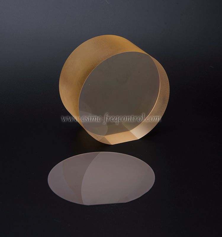
Piezoelectric materials generate an electrical charge when mechanically stressed and deform when an electric field is applied. A piezoelectric wafer uses this effect in resonators, filters, oscillators, surface acoustic wave (SAW) devices, bulk acoustic wave (BAW) components, sensors, actuators, and timing modules.
The wafer is not simply a substrate. Its crystal structure, cut angle, dielectric constant, coupling coefficient, acoustic velocity, loss tangent, thermal expansion coefficient, and surface quality all influence the final component.
For example:
The correct choice depends on the complete device architecture. A material with a high coupling coefficient may still be unsuitable if its temperature coefficient, dielectric loss, or thermal expansion does not match the package and operating environment.
Piezoelectricity was identified in the nineteenth century, but commercial use expanded significantly with the development of quartz oscillators, sonar systems, ceramic transducers, and radio-frequency filters. Later, semiconductor manufacturing introduced wafer-level polishing, photolithography, thin-film metallization, dicing, and batch processing to piezoelectric device production.
This evolution created a more demanding procurement environment. Buyers now specify not only material chemistry but also:
As a result, Common Material Selection Mistakes in Piezoelectric Wafer Procurement are often specification mistakes rather than simple purchasing mistakes. A buyer may order a chemically correct wafer that still fails in the actual process because the orientation, thickness mode, electrode system, or thermal behavior is wrong.
One of the most frequent errors is selecting a material because it is popular in the industry. “Lithium tantalate” or “PZT” is not a complete technical specification. The buyer must define the device mode and required performance first.
Important questions include:
For example, Lithium Tantalate Wafers may be highly suitable for a SAW filter, while a PZT ceramic may be more appropriate for a high-displacement actuator. Selecting the wrong material family can result in low signal amplitude or unacceptable insertion loss even when the wafer appears visually perfect.
Piezoelectric behavior is anisotropic. This means that the electrical and mechanical response changes according to the crystal direction. Wafer labels such as X-cut, Y-cut, Z-cut, 36° rotated Y-cut, or other proprietary orientations must be connected to the device design.
A wrong cut can change:
Before placing an order, CQT engineers should request an orientation certificate or X-ray diffraction verification where appropriate. A drawing should state the reference flat or notch direction, angular tolerance, and crystal-axis convention. “Standard orientation” is not sufficiently precise for a production program.
Thickness is important, but it is only one part of wafer geometry. In acoustic devices, a variation of just a few micrometers can shift resonance frequency and create nonuniformity across the wafer.
A robust purchase specification may include:
| Parameter | Example requirement | Why it matters |
|---|---|---|
| Diameter | 100 mm ± 0.10 mm | Controls tool compatibility and usable wafer area. |
| Thickness | 500 µm ± 5 µm | Influences resonance and mechanical stiffness. |
| TTV | ≤ 3 µm, according to drawing | Improves frequency uniformity across the wafer. |
| Surface roughness | Ra ≤ 1 nm where required | Supports bonding, metallization, and photolithography. |
| Edge exclusion | Defined in millimeters | Prevents defects from entering active die areas. |
These values are examples, not universal requirements. The final limits must be based on the device process. However, specifying dimensional accuracy to 0.01 mm where the process requires it is much safer than using vague terms such as “standard wafer thickness.”
Temperature affects acoustic velocity, dielectric properties, package stress, and resonance frequency. A material that works at room temperature may fail in an automotive, aerospace, telecom, or industrial environment.
Procurement teams should compare:
For lithium tantalate and lithium niobate, the selected crystal cut and package design can be as important as the nominal material itself. A wafer may meet room-temperature electrical specifications but show unacceptable frequency drift after thermal cycling.
A high piezoelectric coefficient does not automatically produce a better component. Device performance is a balance among coupling, dielectric loss, mechanical quality factor, acoustic attenuation, leakage, thermal stability, and electrode geometry.
For instance, a sensor may benefit from high sensitivity, while a frequency reference may prioritize low aging and a high quality factor. An RF filter may require controlled coupling and low insertion loss rather than maximum displacement.
When comparing materials, CQT should review the complete property set instead of focusing on one number:
Wafer procurement sometimes focuses on material certificates while neglecting polishing quality. Scratches, pits, edge chips, crystal pull-out, subsurface damage, and particles can reduce yield during lithography, bonding, electrode deposition, and dicing.
A complete incoming inspection should define:
For critical production, specify 100% visual inspection and a documented sampling plan for dimensional and electrical testing. A supplier should also provide lot identification, inspection records, and a certificate of conformance.
Standards improve communication, but they must be applied correctly. Not every semiconductor wafer standard is automatically suitable for a piezoelectric crystal.
Useful references may include:
Dimensional, crystallographic, and electrical acceptance criteria should also be written into the purchase drawing. A supplier may reference an internal standard, but CQT should confirm the test method, equipment accuracy, sample size, and acceptance limit before approval.
Start with the final application rather than the supplier catalog. Create a matrix linking application requirements to wafer properties.
| Application requirement | Material property to review | Verification method |
|---|---|---|
| Stable RF frequency | TCF, Q factor, aging | Resonance testing across temperature |
| High sensor sensitivity | Piezoelectric coefficient and coupling | Electrical and dynamic characterization |
| Wafer bonding | Flatness, roughness, particles | Surface metrology and microscopic inspection |
| High-temperature operation | Thermal stability and package compatibility | Thermal cycling and aging tests |
A technically suitable material can still create production problems if the supplier cannot maintain lot consistency. Review crystal growth capability, wafer slicing, lapping, polishing, cleaning, packaging, and traceability.
Ask for:
For time-sensitive programs, a documented 24-hour response target for quality issues can reduce line stoppage risk. This is a procurement control, not a substitute for technical qualification.
Do not approve a new wafer material solely from a datasheet. Use a pilot lot to evaluate actual process behavior, including:
Record baseline results and compare at least three lots when possible. This helps separate a material problem from a one-time supplier variation.
Consider a hypothetical CQT project developing a high-frequency SAW filter. The initial purchasing specification requests lithium tantalate wafers with the correct diameter and nominal thickness. The wafers pass visual inspection, but the finished filter shows a wide frequency distribution and excessive insertion loss.
The investigation identifies three linked causes:
The corrective action is to revise the specification for Lithium Tantalate Wafers by adding orientation tolerance, TTV, roughness, edge exclusion, defect classification, and lot-based acoustic verification. After pilot qualification, the production team observes tighter frequency distribution and improved die yield.
This example illustrates why Common Material Selection Mistakes in Piezoelectric Wafer Procurement often appear late in manufacturing. The material name was correct, but the functional and geometric requirements were incomplete.
Unit price does not include scrapped wafers, rework, qualification time, production interruptions, or field returns. A slightly higher wafer price may be financially better if it improves yield and lot consistency.
A datasheet usually presents typical values, not guaranteed values. CQT should distinguish between typical, minimum, maximum, and tested-on-each-lot data.
Growth method, impurity concentration, crystal cut, polishing process, annealing history, and packaging can create major performance differences between suppliers.
Coupling must be balanced with Q factor, loss, thermal behavior, mode purity, and circuit requirements. The best material is the one that meets the full system specification.
Before approving a piezoelectric wafer supplier, confirm the following:
The central lesson from Common Material Selection Mistakes in Piezoelectric Wafer Procurement is simple: do not buy a wafer by material name alone. Match the crystal, cut, dimensions, surface condition, thermal behavior, and test method to the device architecture and manufacturing process.
For CQT programs involving Lithium Tantalate Wafers, a controlled specification, pilot-lot qualification, documented inspection, and standards-based verification can prevent frequency instability, low yield, and expensive redesigns. Engineers and purchasing teams should review every requirement before volume release and work with suppliers that provide measurable data, complete traceability, and fast technical support.
By addressing these common material selection errors early, manufacturers can improve device reliability, shorten qualification cycles, and build a more predictable piezoelectric wafer supply chain.


Copyright © Hangzhou Freqcontrol
Electronic Technology Ltd.
All Rights Reserved | Sitemap |
Powered by 







 中文


