Single Crystal Quartz Wafers are precision quartz substrates used in sensors, optical devices, microfluidics, and semiconductor research. Their stable electrical insulation, low thermal expansion, and strong resistance to many chemicals make them useful where ordinary glass may fail. Buyers comparing a single crystal quartz wafer for sensor devices, high-purity quartz wafer substrates for research, or fused quartz wafers for semiconductor processing must look beyond thickness and diameter. Crystal orientation, surface finish, particle control, and inspection data all affect device performance and production yield.
Choosing the wrong wafer can cause poor bonding, unstable frequency response, surface defects, or contamination during later processing. This guide explains what Single Crystal Quartz Wafers are, how they are made and cleaned, where they are used, and how to select a suitable product from suppliers such as CQT.
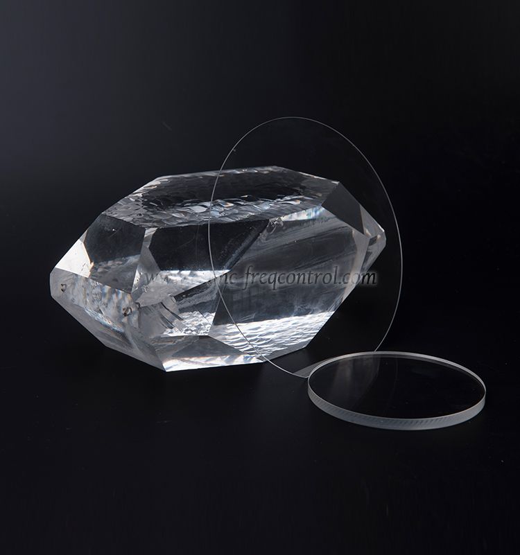
Single Crystal Quartz Wafers are thin, flat slices cut from a single crystal of quartz, usually high-purity crystalline silicon dioxide, or SiO2. Unlike polycrystalline materials, a single crystal has an ordered atomic structure across the wafer. This structure gives the wafer more predictable optical, electrical, thermal, and mechanical behavior.
Quartz is also known as crystalline silica. It should not be confused with fused quartz. Fused quartz is usually an amorphous, non-crystalline form of SiO2. Both materials can provide high purity and good thermal stability, but their crystal structure and functional properties are different.
The final wafer quality depends on each step in the manufacturing chain. A supplier should be able to explain the material source, cutting method, polishing process, cleaning method, and inspection plan.
Manufacturers begin with a suitable quartz crystal. The required grade depends on the application. Optical devices may require low absorption and low scattering. Resonators may require controlled crystal orientation and stable electromechanical behavior. Laboratory substrates may focus on surface quality, flatness, and chemical compatibility.
Material specifications can include:
X-ray diffraction, optical methods, or orientation fixtures may be used to identify the crystal direction. The crystal is then sliced with a diamond blade, wire saw, or another precision cutting system. Cutting creates saw marks and a damaged layer near the surface, so the wafer is normally thicker than the final target at this stage.
For piezoelectric devices, even a small orientation error can change the electrical and temperature response. The acceptable angle tolerance should therefore be stated on the drawing or purchase specification rather than left as a general request for “quartz wafer.”
The wafer edge may be rounded, chamfered, or formed according to the handling system. Edge shaping reduces the chance of chipping during transport and automated loading.
Lapping removes saw damage and brings the wafer closer to its final thickness. This step also improves parallelism. However, lapping alone does not create the low-defect surface needed for advanced coating or bonding.
Polishing uses controlled abrasives and pads to create a smoother surface. Depending on the product, the supplier may offer single-side polishing or double-side polishing.
Ask for measured surface roughness, TTV, flatness, and inspection limits. “Mirror polished” is not a complete technical specification because suppliers may use different inspection methods and acceptance limits.
After polishing, the wafer is cleaned to remove particles, abrasive residue, organic material, and ionic contamination. It may then be inspected under controlled lighting or with particle measurement equipment.
Packaging should protect the polished surface from contact, moisture, dust, and electrostatic attraction. For sensitive processes, wafers may be packed in clean containers or sealed bags and handled with wafer-grade tools.
Cleanliness is not only a visual issue. A particle can block a lithography feature, create a pinhole in a coating, or form a weak point in a bonded interface. Trace metals and organic residues can also interfere with sensors, thin films, and semiconductor process steps.
| Contamination type | Possible effect | Typical control method |
|---|---|---|
| Particles | Defective patterns, poor bonding, optical scattering | Filtered cleaning, cleanroom handling, particle inspection |
| Metal ions | Electrical leakage, altered surface chemistry, device drift | High-purity chemicals, controlled equipment, laboratory analysis |
| Organic residue | Coating adhesion problems and outgassing | Solvent cleaning, oxidizing cleans, controlled drying |
| Water marks | Uneven coating and bonding defects | High-quality rinsing, spin drying, and sealed packaging |
| Scratches and chips | Cracks, stress concentration, and reduced yield | Edge protection, visual inspection, and surface metrology |
There is no single global cleanliness limit that applies to every quartz wafer. The correct limit depends on the device process and customer specification. However, several recognized standards help define the production environment and test method:
When requesting a quotation, specify the particle size and count limit, cleaning method, packaging class, allowable metal contamination, and inspection report format. This prevents different suppliers from using the same word, such as “clean,” to describe different quality levels.
Quartz has piezoelectric behavior. When an electric field is applied, the crystal can deform. When the crystal is mechanically stressed, it can generate an electrical signal. This property supports quartz resonators, oscillators, filters, and timing references.
In these devices, the crystal cut, thickness, electrode design, and temperature compensation method influence the operating frequency. A thickness-shear resonator, for example, requires a tightly controlled wafer thickness and surface condition.
Quartz wafers are used in acoustic sensors, pressure-related research, chemical sensors, biosensors, and microfluidic platforms. Quartz can provide electrical insulation and a stable surface for electrodes or functional coatings.
For biosensor work, surface chemistry is especially important. Researchers may add gold electrodes, silane layers, antibodies, polymers, or other receptor materials. Organic residue or particles on the quartz can reduce coating adhesion and create inconsistent test results.
High-purity quartz is used in optical components because it can transmit light across a broad wavelength range, depending on grade, thickness, surface finish, and impurity level. It may support optical windows, waveguide research, ultraviolet applications, and photonic structures.
Optical users should request transmission data at the intended wavelength instead of relying only on a general purity statement. Surface scattering, absorption bands, coating quality, and internal stress can all affect optical performance.
Quartz wafers can serve as insulating substrates for metal deposition, dielectric films, graphene research, transparent electrodes, and other experimental structures. Their chemical resistance and thermal stability make them useful in selected wet and dry process steps.
Before using a quartz wafer in a semiconductor process, confirm compatibility with:
Universities and development laboratories use quartz substrates for microscopy, electrochemistry, optical experiments, and prototype device fabrication. In these settings, a standard diameter and documented surface condition can reduce setup time and improve repeatability between experiments.
Quartz is an electrical insulator with useful dielectric behavior. This makes it suitable for experiments and devices where the substrate must not conduct current between electrodes.
Quartz has a low coefficient of thermal expansion compared with many common materials. This helps reduce dimensional change during heating and cooling. The actual behavior depends on crystal direction, cut, temperature range, and product grade, so the supplier should provide the relevant data sheet.
Quartz resists many acids and process chemicals, although it is not immune to every chemical. Hydrofluoric acid and strongly alkaline conditions can attack silica-based materials. A chemical compatibility review is required before production use.
Selected quartz orientations support stable resonant behavior. This is one reason quartz remains important in timing and frequency-control applications.
High-purity quartz can provide strong transmission in selected ultraviolet, visible, and infrared ranges. Transmission depends on impurities, thickness, surface finish, and wavelength. A measured transmission curve is more useful than a general claim such as “high transparency.”
A well-controlled wafer specification can reduce variation in coating thickness, bonding quality, etch behavior, and device testing. The benefit comes from measurable controls such as TTV, flatness, roughness, particle count, and orientation tolerance.
State whether the wafer will be used for a resonator, optical component, MEMS device, thin-film process, chemical sensor, or laboratory experiment. Each application requires a different balance of crystal orientation, surface quality, thickness, and cleanliness.
Do not select a cut only by habit. Confirm the required vibration mode, optical axis, piezoelectric response, and temperature behavior. If the wafer is for a resonator, provide the target frequency range and electrode structure to the supplier.
Include the following information in the drawing or request for quotation:
Specify roughness, scratches, stains, chips, particles, and packaging requirements. If the wafer will be bonded or coated, surface roughness and particle limits are often more important than a basic visual inspection.
Useful documents include a certificate of conformity, material or crystal orientation report, dimensional inspection report, surface roughness data, particle inspection results, and cleaning or packaging statement.
Before ordering production quantities, test a sample batch in the actual process. Check coating adhesion, etch response, contact angle, bonding voids, frequency stability, optical transmission, or other application-specific results. A wafer that looks acceptable may still fail during deposition or bonding.
Possible causes include a sharp edge, hidden edge chip, excessive thermal stress, or unsuitable handling tools. Request a defined edge profile, use vacuum or soft-contact tools, and avoid rapid temperature changes.
Surface particles, organic residue, high roughness, or an unsuitable pre-clean may be responsible. Confirm the cleaning process and run a contact-angle or adhesion test before changing the coating chemistry.
Frequency variation can result from thickness variation, crystal-angle error, electrode geometry, temperature, or surface stress. For resonator applications, review thickness mapping and orientation data instead of checking only the nominal thickness.
Check the wavelength, wafer thickness, surface reflection, contamination, internal inclusions, and measurement setup. Ask for a wavelength-specific transmission curve and confirm whether the value includes surface reflection losses.
Particles may come from the cleaning tank, rinse water, drying system, packaging material, or operator handling. Review the complete process, including final rinse quality, drying time, container cleanliness, and time between cleaning and sealing.
| Substrate | Main strengths | Points to review |
|---|---|---|
| Single crystal quartz | Piezoelectric response, electrical insulation, chemical resistance, low thermal expansion | Crystal orientation, cut angle, cost, chemical compatibility |
| Fused quartz | High thermal stability, optical use, amorphous structure | Does not provide the same single-crystal piezoelectric behavior |
| Silicon | Strong semiconductor manufacturing infrastructure and process availability | Electrical behavior, thermal expansion, and chemical response differ from quartz |
| Sapphire | High hardness, optical use, and strong thermal performance | Different dielectric, optical, and crystal properties; can be harder to process |
| Glass | Low cost and easy availability | Amorphous structure and performance may not meet precision resonator needs |
No. Single crystal quartz has an ordered crystal lattice and can provide orientation-dependent piezoelectric behavior. Fused quartz is generally amorphous. The correct choice depends on whether the application needs crystal orientation and resonant performance.
Yes, quartz wafers can be used as insulating substrates for selected deposition, lithography, etching, and research processes. Confirm the chemical, thermal, plasma, vacuum, and particle requirements before production use.
There is no single value for every application. Optical windows, thin-film deposition, direct bonding, and laboratory testing may require different roughness levels. Specify the required Ra or RMS value and the measurement method.
Quartz is anisotropic, which means its properties change with direction. Orientation affects piezoelectric response, resonant frequency, thermal behavior, optical behavior, and mechanical performance.
Use a cleaning process compatible with the wafer grade and the next process step. A typical process may include particle removal, solvent cleaning, high-purity water rinsing, controlled drying, inspection, and clean packaging. Avoid hydrofluoric acid unless the process has been specifically designed and validated for it.
Keep them in sealed, clean packaging in a low-particle environment. Do not place polished surfaces directly against hard materials. Follow the supplier’s instructions for temperature, humidity, shelf life, and unpacking.
CQT can be contacted to discuss application-specific requirements such as crystal orientation, diameter, thickness, polishing, edge shape, cleanliness, and packaging. Send a technical drawing or sample specification to receive a more accurate recommendation.
Single Crystal Quartz Wafers support frequency control, sensors, optical systems, thin-film research, and other precision applications. Their value comes from measurable properties: crystal orientation, thickness uniformity, surface roughness, flatness, chemical compatibility, and cleanliness. Start by defining the device process, then request a wafer drawing, inspection limits, cleaning statement, and sample batch.
For a practical next step, review your process conditions and prepare a specification covering diameter, thickness, cut angle, polish, TTV, surface roughness, particle limits, and packaging. Then contact CQT for a product discussion or trial order. Testing a small batch in the real process is the most reliable way to confirm that the selected high-purity quartz wafer substrate for research and production meets your performance and yield targets.


Copyright © Hangzhou Freqcontrol
Electronic Technology Ltd.
All Rights Reserved | Sitemap |
Powered by 







 中文


