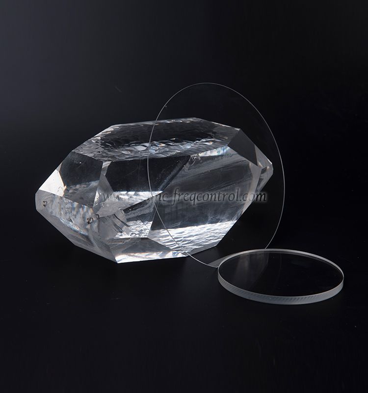
Single Crystal Quartz Wafers are selected for frequency control, timing, sensors, optical devices, and other applications that require stable electrical and mechanical performance. Purchasing teams searching for aging and stability information usually want more than a material definition. They need a clear method to compare wafer specifications, identify long-term drift risks, validate supplier data, and prevent performance failures after production.
Start by defining the stability requirements before choosing a wafer
Identify the performance value that must remain stable
Aging is not a single pass or fail characteristic. The relevant stability target depends on the final application and the way the wafer will be processed. Before requesting quotations, define the electrical, mechanical, optical, and environmental values that must remain within limits.
- Resonant frequency or frequency-temperature behavior.
- Frequency drift over a specified time period.
- Equivalent series resistance after processing.
- Crystal orientation and cut accuracy.
- Wafer thickness and thickness uniformity.
- Surface roughness and polishing quality.
- Particle level and metallic contamination.
- Breakage rate during dicing, cleaning, bonding, or packaging.
- Performance after humidity, temperature cycling, vibration, or storage.
Separate short-term stability from long-term aging
Short-term stability describes the response to immediate changes such as temperature, drive level, mounting stress, and handling. Long-term aging describes the gradual change that occurs during storage and operation. A wafer can show good initial test data and still experience unacceptable drift if residual stress, contamination, surface damage, or packaging effects are not controlled.
Ask the supplier to identify whether each reported value represents:
- Initial wafer inspection.
- Post-cleaning inspection.
- Post-processing inspection.
- Accelerated aging data.
- Real-time aging data.
- Data from a finished resonator or data from the bare wafer.
Convert application needs into purchasing specifications
The purchasing group should convert engineering requirements into measurable acceptance criteria. This prevents suppliers from quoting different materials under the same general product name.
- Record the required crystal type and cut, such as AT cut, BT cut, or another application-specific orientation.
- Define wafer diameter, thickness, thickness tolerance, and usable area.
- Specify surface finish, roughness, flatness, total thickness variation, and edge condition.
- Set limits for particles, stains, scratches, chips, cracks, and inclusions.
- Define allowable frequency drift or dimensional change after the required aging period.
- Specify the test temperature, humidity, drive condition, mounting method, and measurement equipment.
- Require a certificate of analysis and a traceable lot number for every shipment.
Understand the main physical causes of aging in quartz wafers
Residual stress can create gradual performance drift
Mechanical stress may remain after cutting, grinding, lapping, polishing, cleaning, or wafer handling. This stress can slowly relax during storage or operation. When the stress state changes, the resonant, dimensional, or optical behavior of the quartz component may also change.
Common sources of residual stress include:
- Excessive grinding or lapping pressure.
- Uneven polishing across the wafer.
- Improper edge preparation.
- Thermal shock during cleaning or drying.
- Mechanical clamping during inspection.
- Incorrect bonding or mounting conditions.
Surface damage can become a long-term reliability problem
Microcracks, subsurface damage, scratches, and chipped edges may not cause immediate rejection during visual inspection. However, these defects can grow during thermal cycling, vibration, handling, or device assembly. Surface damage can also increase contamination retention and make cleaning less effective.
Purchasing teams should request inspection criteria for:
- Front-side and back-side scratches.
- Polishing haze and cloudy areas.
- Edge chips and edge fractures.
- Visible cracks under magnification.
- Subsurface damage detected by appropriate inspection methods.
- Particles attached after final cleaning.
Contamination can change stability after assembly
Organic residues, alkali ions, metal particles, and process chemicals can remain on the wafer surface. These contaminants may affect bonding, electrode adhesion, leakage behavior, surface charge, or long-term frequency stability. A wafer that is clean at shipment can become contaminated if packaging, storage, or handling controls are weak.
Important contamination controls include:
- Final cleaning chemistry and rinse quality.
- Drying method and drying temperature.
- Cleanroom classification during packing.
- Packaging material compatibility.
- Operator glove and tool control.
- Particle and ionic contamination testing.
Compare the wafer parameters that influence long-term stability
Check crystal type, cut, orientation, and uniformity
Crystal orientation directly affects temperature behavior, elastic response, vibration mode, and manufacturability. The purchasing specification should state the required cut and orientation rather than using only the phrase quartz wafer.
Request the following information:
- Quartz material grade and crystal type.
- Cut angle and orientation tolerance.
- Wafer diameter and thickness.
- Thickness uniformity across the wafer.
- Orientation marking method.
- Crystal defect inspection method.
- Lot-to-lot consistency records.
Evaluate thickness, flatness, and surface roughness
Thickness variation can affect resonance, mechanical response, etching uniformity, and yield. Flatness and total thickness variation are especially important when the wafer will be bonded, patterned, coated, or processed in automated equipment.
Useful purchasing parameters include:
- Nominal thickness.
- Thickness tolerance.
- Total thickness variation.
- Bow and warp.
- Surface roughness value and measurement method.
- Flatness over the usable area.
- Edge exclusion zone.
- Maximum allowable scratches, pits, stains, and particles.
Do not judge aging risk from initial frequency data alone
Initial frequency or dimensional measurements show the condition of the wafer at one point in time. They do not prove long-term stability. A reliable evaluation combines initial data with environmental exposure, repeated measurement, and process simulation.
Request test records that show:
- Measurement repeatability.
- Measurement equipment calibration status.
- Preconditioning procedure.
- Storage time before measurement.
- Temperature and humidity during measurement.
- Drift trend over time.
- Failure or rejection criteria.
Use a step-by-step incoming inspection process
First step: prepare the required tools and documents
Incoming inspection should be performed with equipment that matches the wafer specification. Record the instrument identification and calibration status so that results can be traced to a specific inspection event.
Required tools may include:
- Cleanroom gloves, face covering, hair covering, and protective clothing.
- Certified wafer handling tweezers or vacuum wand.
- Particle-controlled wafer trays and storage boxes.
- Optical microscope with suitable magnification.
- Dark-field and bright-field lighting.
- Surface profilometer or roughness measurement instrument.
- Thickness gauge or noncontact thickness measurement system.
- Flatness, bow, and warp measurement system.
- Cleanroom scale if mass control is required.
- Temperature and humidity monitor.
- Data recording software or a controlled inspection form.
- Calibration certificates and the supplier certificate of analysis.
Second step: verify packaging and traceability
- Confirm that the outer package is intact and free of moisture damage.
- Record the supplier name, product code, wafer size, lot number, quantity, and shipment date.
- Compare the label with the purchase order and certificate of analysis.
- Check whether the packaging is sealed and whether the seal shows evidence of tampering.
- Move the unopened package into the controlled inspection area before opening it.
Third step: inspect the wafer visually
- Put on cleanroom gloves and use approved wafer handling tools.
- Open the package in a controlled environment.
- Inspect both surfaces under bright-field lighting.
- Inspect the wafer under dark-field lighting to reveal particles and fine scratches.
- Check the edge for chips, cracks, sharp areas, and handling marks.
- Inspect the orientation mark and compare it with the order specification.
- Record the location and size of every nonconformity.
Fourth step: measure geometry and surface condition
- Measure wafer diameter and compare it with the approved drawing.
- Measure thickness at the center and at defined points near the edge.
- Calculate thickness variation across the wafer.
- Measure bow, warp, and flatness using the approved method.
- Measure surface roughness at representative locations.
- Compare the results with the purchase specification and supplier certificate.
- Quarantine any lot that exceeds limits until engineering review is complete.
Fifth step: perform stability screening when the application is sensitive
- Select representative wafers from the lot according to the sampling plan.
- Record baseline measurements under controlled temperature and humidity.
- Expose the samples to the defined storage, temperature cycling, humidity, or vibration condition.
- Return the samples to the reference condition before the next measurement.
- Repeat the same measurement method at each interval.
- Plot the change against time rather than comparing only the beginning and end values.
- Investigate sudden changes separately from gradual drift.
Build an accelerated aging and stability test plan
Define the test objective and test condition
An accelerated test is useful only when the condition represents a credible failure mechanism. Excessive temperature or humidity may create a failure mode that does not occur in normal service, while a weak test may not reveal meaningful drift.
Define the following before testing:
- Test objective, such as screening contamination, stress relaxation, or packaging risk.
- Number of wafers and number of lots.
- Initial measurement method.
- Environmental exposure condition.
- Exposure duration.
- Measurement intervals.
- Recovery time before measurement.
- Acceptance limits and escalation rules.
Measure a baseline before exposure
- Condition the wafer samples in the reference environment.
- Clean and handle all samples using the same approved procedure.
- Measure geometry, surface condition, and application-specific performance.
- Repeat critical measurements to establish instrument repeatability.
- Record operator, instrument, date, temperature, humidity, and sample location.
Apply environmental exposure without introducing test artifacts
- Place the samples in a fixture that does not apply unexpected mechanical stress.
- Prevent samples from touching each other or contaminated chamber surfaces.
- Record actual chamber temperature and humidity, not only the programmed values.
- Inspect the chamber for condensation, chemical residue, or contamination.
- Use control samples when possible.
- Document every interruption, power failure, or chamber excursion.
Analyze the drift trend and make a purchasing decision
Use the trend to classify the lot instead of relying on a single final reading. A gradual and repeatable change may indicate normal aging, while a sudden change may indicate handling damage, contamination, thermal shock, or measurement error.
Recommended decision categories are:
- Approved: results remain within limits with a stable trend.
- Conditionally approved: results are acceptable but require tighter process controls.
- Engineering review: results show unexplained variation or a weak trend.
- Rejected: results exceed the defined stability or quality limits.
Control storage, handling, and processing after receipt
Use a controlled storage procedure
- Store wafers in clean, sealed containers designed for wafer protection.
- Keep the storage area within the temperature and humidity range specified by engineering.
- Protect wafers from direct sunlight, chemical vapors, vibration, and rapid temperature changes.
- Use first-in, first-out inventory control unless the qualification plan requires another method.
- Record opening dates and exposure time for each package.
- Reseal unused wafers immediately after removal.
- Reinspect aged or repeatedly opened packages before production use.
Handle wafers without adding mechanical or chemical damage
- Touch only approved handling areas.
- Never slide one wafer across another wafer or across a hard tray surface.
- Do not stack wafers without a qualified separator.
- Use clean tools with rounded contact surfaces.
- Avoid excessive vacuum force or point loading.
- Keep cleaning chemistry, rinse water, and drying parameters consistent.
- Minimize the time between final cleaning and packaging or assembly.
Control downstream processes that can create apparent aging
Some changes attributed to wafer aging are actually caused by assembly or process conditions. Bonding stress, electrode deposition, thermal treatment, adhesives, fixtures, and packaging can alter the final performance.
Review these process variables:
- Bonding temperature and pressure.
- Adhesive type, cure schedule, and outgassing behavior.
- Electrode material and deposition energy.
- Cleaning and plasma treatment conditions.
- Etching depth and profile.
- Fixture alignment and clamping force.
- Final package moisture and gas composition.
Qualify a supplier that can control aging risk
Request evidence of process control
A purchasing decision should consider process capability, not only the lowest unit price. Ask the supplier to explain how crystal growth, cutting, lapping, polishing, cleaning, inspection, and packing are controlled.
Useful supplier evidence includes:
- Material and crystal orientation documentation.
- Process flow diagram.
- Inspection plan and sampling method.
- Calibration and measurement system records.
- Lot traceability procedure.
- Nonconforming product control process.
- Corrective action records for previous quality issues.
- Stability or aging test data from comparable wafer designs.
- Packaging and storage recommendations.
Compare suppliers using a weighted scorecard
A weighted scorecard helps the purchasing group compare suppliers on total risk rather than price alone.
- Material consistency and crystal orientation control.
- Thickness, flatness, and surface roughness capability.
- Particle and contamination control.
- Stability test quality and data transparency.
- Lot traceability and certificate accuracy.
- Production capacity and delivery reliability.
- Technical support and response time.
- Corrective action speed and communication quality.
- Total cost of ownership, including yield loss and retesting.
Use a qualification lot before approving regular supply
- Send the supplier a controlled drawing and complete specification.
- Request samples from a normal production lot rather than a specially selected demonstration lot.
- Perform incoming inspection using the same method planned for production.
- Process the wafers through representative cleaning, bonding, coating, or dicing steps.
- Perform application-specific stability testing.
- Review defects, yield, drift, and process compatibility with engineering and quality teams.
- Approve the supplier only after all critical criteria pass.
- Continue periodic lot audits after approval.
Avoid common mistakes that hide wafer aging problems
Mistake one: accepting a generic specification
The phrase high purity quartz wafer does not define orientation, thickness uniformity, surface quality, contamination limits, or aging performance. Require a controlled drawing and measurable acceptance criteria.
Mistake two: testing only one wafer from one lot
One sample cannot represent lot variation. Use a sampling plan that covers multiple wafer locations and, when practical, multiple production lots.
Mistake three: confusing measurement error with material aging
Changes may result from temperature variation, instrument drift, operator technique, fixture stress, or inconsistent cleaning. Repeat measurements under controlled conditions before concluding that the wafer has aged.
Mistake four: skipping post-process testing
Bare wafer results may not predict finished device behavior. Include representative assembly and packaging steps when those processes can introduce stress, contamination, or thermal exposure.
Mistake five: storing wafers in uncontrolled packaging
Open trays, unsuitable plastics, paper fibers, and repeated handling can increase particles and chemical contamination. Use qualified containers and record package opening history.
Mistake six: using an accelerated test without a failure model
Extreme test conditions may produce misleading results. Define the suspected aging mechanism and select a test condition that can reveal it without creating an unrelated failure mode.
Mistake seven: selecting a supplier based only on initial price
Low purchase price can be offset by unstable lots, yield loss, delayed deliveries, additional inspection, and field failures. Include long-term process risk in the supplier evaluation.
Use a practical purchasing checklist for Single Crystal Quartz Wafers
Checklist for the technical specification
- Crystal material and grade.
- Required cut and orientation.
- Wafer diameter and thickness.
- Thickness tolerance and total thickness variation.
- Flatness, bow, and warp limits.
- Surface roughness and polishing condition.
- Particle, scratch, pit, stain, crack, and chip limits.
- Edge exclusion and orientation marking.
- Packaging and storage requirements.
- Required certificate of analysis and traceability data.
Checklist for the aging and stability plan
- Define the performance value to be monitored.
- Record a controlled baseline.
- Use representative samples from multiple lots when possible.
- Control temperature, humidity, handling, and mounting conditions.
- Measure at planned intervals.
- Separate gradual drift from sudden failure.
- Compare bare wafer data with post-process data.
- Document acceptance limits and corrective actions.
Checklist for supplier communication
- Provide the supplier with the complete technical drawing.
- Ask for normal production samples and historical stability data.
- Confirm the supplier's inspection methods and calibration controls.
- Confirm lot traceability from material through packaging.
- Agree on change notification requirements.
- Define nonconformance response time.
- Review storage life and recommended handling conditions.
For buyers, the safest approach is to treat aging as a system-level risk involving crystal quality, wafer geometry, surface condition, contamination, handling, processing, packaging, and measurement. CQT can support a controlled evaluation of Single Crystal Quartz Wafers by helping customers align wafer specifications, inspection requirements, stability testing, and supplier qualification with the final application.









 中文


