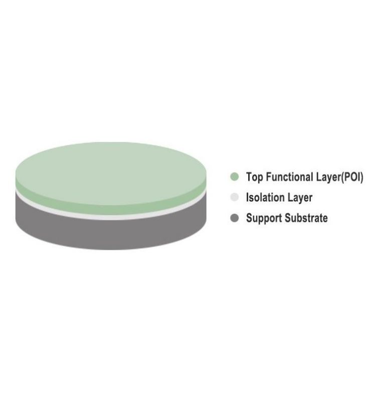


Lithium Niobate Thin Films on Insulator is kind of POI (Piezoelectric on Insulator) wafer. It's stacked sequence structure is made of support substrates that can be silicon, quartz, fused silica, sapphire or LN wafer, the interlayer is thermal oxide SiO2 that works as insulator
Lithium Niobate Thin Films on Insulator is kind of POI (Piezoelectric on Insulator) wafer. It’s stacked sequence structure is made of support substrates that can be silicon, quartz, fused silica, sapphire or LN wafer, the interlayer is thermal oxide SiO2 that works as insulator and lithium niobate film is the functional layer above the insulation layer.
POI /LNOI engineered substrates enable the design of filters with high quality factor, large bandwidth, very low temperature sensitivity and low insertion loss with a simple device manufacturing technology. These wafers are developed and used for high-speed modulators, high Q factor SAW devices, IR-detectors, THz devices.
We work with our strategical partner who has experienced at technology of smart cut and wafer bonding and supply with important Piezoelectric layer on LN/LT from the sizes of 3” 4” 6” up to 8” to build the special wafer with multilayered structure.
LNOI substrates provide multiple technical benefits that make them ideal for advanced electronic and photonic devices.
1. High Quality Factor (Q Factor)
Devices fabricated on LNOI wafers demonstrate exceptionally high Q factors, which improves signal stability and performance in RF filters and resonators.
2. Large Bandwidth Performance
The optimized thin-film structure supports high-frequency operation, making LNOI suitable for modern wireless communication technologies such as:
5G
RF front-end modules
Advanced telecom systems
3. Low Insertion Loss
Low signal attenuation ensures efficient signal transmission in optical and RF devices, improving overall device performance.
4. Excellent Temperature Stability
LNOI wafers provide low temperature sensitivity, which is critical for high-precision optical and sensing applications.
5. Simplified Device Fabrication
Compared with traditional bulk materials, LNOI enables:
Smaller device footprints
Higher integration density
CMOS-compatible fabrication processes
This helps reduce manufacturing complexity and production costs.
Specifications For LNOI
Layers | Parameters | Specifications | |||
Top Functional Layer | Material | Lithium Niobate Lithium Tantanlate | |||
Diameter | 3" | 4" | 6" | 8" | |
Surface orientation | X-cut or per request | ||||
Primary flat oritentation | per request | deg(°) | |||
Secondary flat orientation | per request | ||||
Film Thickness average thickness | 300-600 | nm | |||
Front side /face roughness | Optical polished | ||||
Isolation Layer | Buried Oxide avg thickness | 4600 | 4700 | 4800 | nm |
Buried Oxide thickness uniformity | -5 | 0 | 5 | % | |
Support substrate | Material | SI/LN/SAPPHIRE/QUARTZ/ETC | |||
Diameter | 3" | 4" | 6" | 8" | |
Support layer total thickness | 525 | 525 | 625 | 725 | |
Device growth method | CZ | CZ | ZVD | hydrothermal | |
Device orientation | {100} | 0.5 | deg(°) | ||
Device doping type | N | N | |||
Device dopant | Phos | ||||
Surface finish | 10 | nm | |||
The production of LNOI wafers relies on advanced semiconductor fabrication technologies:
Smart-Cut Technology
This process allows the transfer of ultra-thin lithium niobate layers onto insulating substrates with high uniformity and precision.
Wafer Bonding
Wafer bonding techniques create strong, defect-free interfaces between layers, ensuring reliability and performance.
High-Precision Layer Control
The thickness of the lithium niobate thin film and oxide layer can be controlled at nanometer levels, which is essential for photonic device performance.
These processes result in highly reliable engineered wafers suitable for large-scale manufacturing.
LNOI technology is enabling breakthroughs across multiple high-tech industries.
High-Speed Optical Modulators
LNOI is widely used in optical communication systems due to its strong electro-optic effect, enabling:
Ultra-fast data transmission
Low power consumption
Compact photonic integrated circuits
SAW (Surface Acoustic Wave) Devices
High Q-factor SAW devices manufactured on LNOI wafers are used in:
RF filters
Wireless communication equipment
Signal processing systems
Infrared (IR) Detectors
LNOI materials support advanced sensing systems, including:
Infrared imaging
Environmental monitoring
Industrial detection systems
THz Devices
Terahertz technologies are emerging in fields such as:
Security screening
Medical imaging
High-speed wireless communication
LNOI substrates play a key role in enabling these next-generation devices.
Integrated Photonics
Many photonic integrated circuits rely on LNOI wafers for:
Optical switching
Laser systems
Quantum photonics
The demand for faster communication, smaller devices, and higher integration density is pushing semiconductor materials beyond traditional solutions. LNOI wafers provide a unique combination of:
Electro-optic performance
Piezoelectric properties
Integration capability
Scalable manufacturing
As a result, LNOI is rapidly becoming a preferred platform for advanced RF, photonics, and sensing technologies.
Reliable Supply of High-Quality LNOI Wafers
Through collaboration with experienced technology partners specializing in smart-cut and wafer bonding, high-quality piezoelectric layers on LN/LT can be produced with stable performance and excellent wafer consistency.
Available solutions include:
Multilayer engineered POI wafers
Custom substrate selections
Precision thin-film lithium niobate layers
Flexible wafer size options from 3″ to 8″
These capabilities support both research institutions and large-scale semiconductor manufacturing.



Copyright © Hangzhou Freqcontrol
Electronic Technology Ltd.
All Rights Reserved | Sitemap |
Powered by 







 中文
中文


