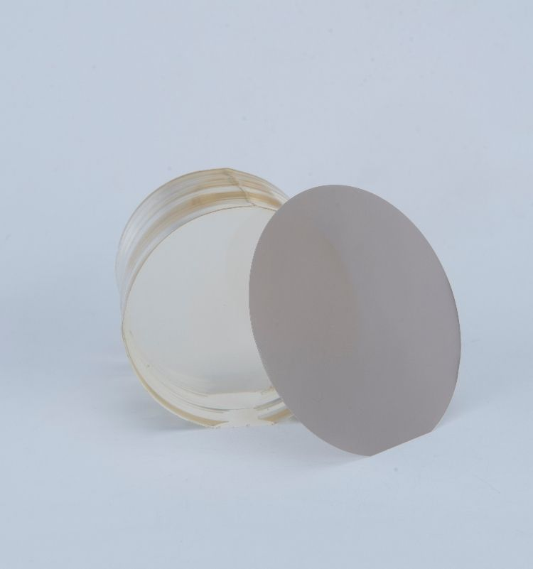
Lithium niobate (LiNbO₃) wafers are high-performance crystalline substrates widely used in advanced electronics and photonics. Their unique combination of optical, piezoelectric, and electro-optic properties makes them indispensable in telecommunications, laser systems, sensors, and emerging photonic devices.
These wafers are precisely sliced from high-quality single crystals and polished to nanometer-level smoothness, providing unmatched stability and performance for critical applications.
Electro-Optic Effect
Lithium niobate exhibits a strong electro-optic effect, meaning it can modulate light in response to electric fields. This property is crucial in optical modulators for fiber-optic communication, enabling high-speed data transfer with minimal signal loss.
Piezoelectricity
The strong piezoelectric response of lithium niobate allows it to convert mechanical energy into electrical signals and vice versa. This makes it suitable for surface acoustic wave (SAW) devices, actuators, and sensors in industrial and aerospace applications.
Optical Transparency
LiNbO₃ wafers are transparent across a wide spectral range (400–5000 nm), making them ideal for laser components, frequency doublers, and nonlinear optical devices. This ensures high efficiency in converting light frequencies without significant losses.
Thermal and Chemical Stability
Lithium niobate maintains performance across wide temperature ranges and resists chemical degradation, making it reliable for high-power laser systems and harsh industrial environments.
Crystal Growth
High-purity lithium niobate crystals are grown using the Czochralski process. Precise control over temperature, rotation speed, and stoichiometry ensures low defect density and uniformity.
Orientation and Cutting
Crystals are oriented along X, Y, or Z axes depending on the target application. This orientation determines the wafer's electro-optic and piezoelectric behavior. Precision diamond saws cut wafers into uniform thicknesses.
Polishing and Surface Treatment
Multi-stage polishing achieves angstrom-level surface smoothness, reducing scattering and enhancing optical performance. Additional chemical-mechanical polishing may be applied for ultra-high-end photonics devices.
Doping and Coating
Doping with magnesium or iron enhances resistance to photorefractive damage, especially for high-power laser applications. Anti-reflection coatings can be added to improve optical throughput.
Telecommunications
Lithium niobate wafers power high-speed optical modulators, enabling rapid data transmission in fiber-optic networks. They are key to 5G infrastructure and next-generation broadband systems.
Consumer Electronics
LiNbO₃ is used in laser scanning, optical sensors, and precision actuators in devices like smartphones, cameras, and VR/AR hardware. Its compact size and high performance make it ideal for portable electronics.
Medical Technology
In laser surgery, diagnostic imaging, and therapeutic devices, lithium niobate ensures precision and reliability. Its optical clarity and electro-optic control are critical for surgical accuracy and patient safety.
Defense and Aerospace
LiNbO₃ wafers are used in high-precision sensors, guidance systems, and satellite communication devices, where environmental stability and robustness are non-negotiable.
X-Cut Wafers: Suitable for acousto-optic devices and frequency shifters.
Y-Cut Wafers: Common in SAW devices and sensors.
Z-Cut Wafers: Ideal for electro-optic modulators and optical phase control.
Magnesium-Doped Wafers: Resistant to photorefractive damage, suitable for high-power lasers.
Thin-Film Lithium Niobate on Insulator (LNOI): Emerging technology for integrated photonics and miniaturized optical circuits.
Application Requirements: Match wafer orientation, thickness, and doping to the device’s functional needs.
Surface Quality: High optical clarity and low roughness reduce signal loss in photonics.
Doping Level: For high-power lasers, magnesium-doped wafers prevent photorefractive damage.
Cost vs. Performance: Balance budget constraints with required performance, especially for precision applications.
Integrated Photonics Growth: Thin-film lithium niobate is driving miniaturization in optical circuits.
5G and Beyond: High-speed optical modulators will see increasing demand.
Quantum Computing Applications: LiNbO₃ wafers are critical for developing quantum photonic devices.
Sustainability and Manufacturing Innovation: Industry is exploring more efficient crystal growth and polishing techniques to reduce waste and production costs.
Lithium niobate wafers are a cornerstone of modern photonics and electronics, offering unparalleled optical, piezoelectric, and electro-optic properties. Their versatility makes them essential across telecommunications, consumer electronics, medical devices, and aerospace applications.
By understanding wafer types, manufacturing processes, and material properties, engineers and buyers can select the optimal solution for their specific needs. With ongoing innovations like LNOI and high-speed modulators, lithium niobate technology will continue to shape the future of high-tech industries.



Copyright © Hangzhou Freqcontrol
Electronic Technology Ltd.
All Rights Reserved | Sitemap |
Powered by 







 中文
中文


